New Trend in Electron Microscopy: Aberration-Corrected Low Voltage TEM
— A Review —
Introduction
This article gives an overview on world-wide activities in Low-Voltage Aberration-Corrected Transmission / Scanning Transmission Electron Microscopy (TEM/STEM) research evaluated on the basis of scientific publications until the end of 2011. At present, Low-Voltage is predominately referring to TEM/STEM <100kV [1]. However, there are three projects, which address the development of microscopy at even lower voltages: SALVE (Germany, with Zeiss NTS, down to 20 kV), Triple-C (Japan, with JEOL Ltd., down to 30 kV), SofTEAM (US, with FEI Electron Optics, project start not yet defined [2]). Our current challenges in low voltage microscopy are I) Optimization of all microscope components for low-voltages <80 kV including the Cs/Cc aberration corrector; II) Applied research, to solve materials science problems, which could not be solved at higher voltages because of radiation damage; III) Basic research, to address questions related to the low voltage TEM instrument on the one hand and imaging, spectroscopy and diffraction modes on the other; IV) Specimen preparation for low voltages; V) Scattering theory at lower voltages; VI) Fulfillment of room requirements (see also in the main menu the topic 'Research'). Such development has been enabled by the achievements on aberration-correction at the end of last century (see our related News articles: 'Wolf Prize' and 'Historical Aspects of hardware aberration correction'). For studies on similiar topics by others see [3-5].
- >> Europe >>
- >> Germany >>
- >> CEOS: Corrected Electron Optical Systems GmbH
- >> Carl Zeiss NTS
- >> IFW: Leibniz Institute for Solid State and Materials Research
- >> MPI for Solid State Research Stuttgart
- >> FZ Jülich
- >> MPI for Biochemistry Martinsried
- >> MPI for Chemical Physics of Solids Dresden
- >> Ulm University >>
- >> Dresden University of Technology >>
- >> University Heidelberg
- >> Technical University Darmstadt
- >> Ilmenau University of Technology
- >> Great Britain >>
- >> SuperSTEM Daresbury
- >> STFC: Science and Technology Facilities Council
- >> University of Oxford >>
- >> University of Nottingham
- >> University of Warwick
- >> University of Manchester
- >> University of Surrey
- >> University of Liverpool
- >> University of Cambridge
- >> Imperial College London
- >> University of Birmingham
- >> University of Salford
- >> Netherlands >>
- >> Finland >>
- >> Switzerland >>
- >> Belgium >>
- >> Austria >>
- >> Italy >>
- >> France >>
- >> Spain >>
- >> Sweden >>
- >> Slovakia >>
- >> Poland >>
- >> Ireland >>
- >> Germany >>
- >> North America >>
- >> USA >>
- >> Nion Corp.
- >> FEI Electron Optics - US
- >> DOW Chemical Company
- >> Carl Zeiss NTS - US
- >> IBM
- >> Quantachrome Instruments
- >> LBNL: Lawrence Berkeley National Laboratory >>
- >> ORNL: Oak Ridge National Laboratory
- >> ANL: Argonne National Laboratory >>
- >> Harvard University / MIT >>
- >> University of California >>
- >> University of Illinois at Urbana Champaign >>
- >> Cornell University >>
- >> University of Texas
- >> Stanford University >>
- >> Lehigh University
- >> Missouri State University
- >> University of Albany
- >> Rice University
- >> University of New Hampshire
- >> University of California Davis
- >> Canada >>
- >> Mexico >>
- >> USA >>
- >> Asia >>
- >> Japan >>
- >> JEOL Ltd.
- >> AIST >>
- >> Tokyo Institute of Technology
- >> NIMS: National Institute for Materials Science >>
- >> CREST: Core Research for Evolutional Science and Technology
- >> ERATO: Nakamura Functional Carbon Cluster Project
- >> Shinshu University
- >> Nagoya University >>
- >> Tokyo Metropolitan University
- >> Meijo University
- >> University of Tokyo
- >> Taiwan >>
- >> Israel >>
- >> Weizmann Institute of Science >>
- >> South Korea >>
- >> China >>
- >> Russia >>
- >> Japan >>
- >> Oceania >>
- >> Australia >>
- >> New Zealand >>

To view the Flash-version of this page ensure that Adobe Flash Player version
10.2.0 or greater is installed.

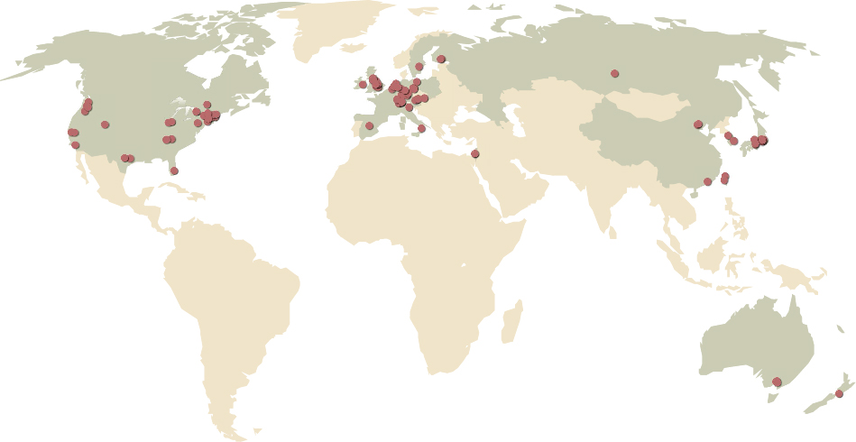
Figure 1: Evaluation of published papers on Low-Voltage Aberration-Corrected TEM/STEM topics until the end of 2011 with respect to their originating institutions and their location on the world map. If you click on a marked continent, its enlarged map appears and you see several red dots as well as a list of countries (Flash-version only). Clicking on this list as well as moving the mouse over the red dots shows the institution names, from which Low-Voltage Aberration-Corrected TEM/STEM papers were published. Clicking on an institutions name in the list directs to the corresponding website. You can find the underlying low-voltage publication list under the main menu 'Publications' >> 'by SALVE authors' and 'by other authors'*.
Europe
With 51% of Europe’s papers published on Hardware Low-Voltage Aberration-Corrected TEM/STEM topics, Germany is an important partner country for application and development of this topic today. The three main institutions in Europe are Ulm University, Electron Microscopy for Materials Science (EMMS) (21%); Leibniz Institute for Solid State and Materials Research (IFW) Dresden (16%); and University of Oxford, Oxford Materials (OM) (14%). It is interesting to note that Germany’s and Great Britain’s institutions all together comprise 79% of Europe’s contribution to Low-Voltage Aberration-Corrected TEM/STEM research. The remaining 21% are distributed as follows: Holland (7%), Finland (5%), Switzerland and Belgium (3%), Austria and Italy (1%), and others (5% all together, see the map).
World-Wide
Europe’s proportion on the total number of Low-Voltage Aberration-Corrected TEM/STEM publications evaluated is 55%. The European SALVE project alone contributes 15%. North American’s proportion on the total number of Low-Voltage Aberration-Corrected TEM/STEM publications evaluated is 30%. The American TEAM project alone contributes 6%. Asia's proportion on the total number of Low-Voltage Aberration-Corrected TEM/STEM publications evaluated is 15%; The Japanese Triple-C project partners alone contribute 8%.
The global country ranking (of the number of publications in Low-Voltage Aberration-Corrected TEM/STEM until 2011) is: USA (29%); Germany (28%); Great Britain (15%); Japan (11%); Netherlands, Finland (3% each); Switzerland (2%); Belgium, Canada, Taiwan, Israel, Austria, China, Australia, Italy, Others (1% each).
The global facility ranking is: Ulm University (12%); Lawrence Berkeley National Laboratory (10%); IfW Dresden (9%); Oxford University (8%); AIST (6%); Harvard University (4%); University of California, JEOL Ltd. and FEI Electron Optics (3% each); University of Helsinki, University of Nottingham, Max Planck Institute for Solid State Research Stuttgart, CEOS GmbH and Nion Corp. (2% each); others (34%), for more details see the world map.
Currently, the most common measurement methods in Low-Voltage Aberration-Corrected Electron Microscopy are: TEM (78%); TEM-STEM (12%); and STEM (10%) (see Fig. 2). In Europe TEM is applied most often (87%); STEM (7%); and TEM-STEM (6%) are used less often. In North-America, TEM is used in 70% of Low-Voltage Aberration-Corrected studies; TEM-STEM in 17%; and STEM in 13%. In Asia TEM is used in 58% of LV AC studies; while TEM-STEM and STEM are used in 22% and 20% respectively (see Fig. 3).
The most studied materials by Low-Voltage Aberration-Corrected TEM/STEM in 114 publications (note that publications using test-specimen are not included): Low-D Carbon Materials (48%); Functionalized graphene/CNT/fullerene including Metallo-Fullerenes (22%); Low-D Inorganic Materials (12%); Nanocrystals (8%); Oxydes, Biological Materials (4% each); Semiconductors (2%) (see Fig. 4).
The most studied materials in the three low-voltage development projects (including test-specimen) are: SALVE (48% Low-D Carbon Materials, 25% Functionalized graphene/CNT/fullerene, 16% Test-Specimen, 11% others); TEAM (35% Low-D Carbon Materials, 29% Test-Specimen, 12% Functionalized graphene/CNT/fullerene, 11% Nanocrystals, 13% others); and the Triple-C Project (48% Test-Specimen, 24% Low-D Carbon Materials, 17% Functionalized graphene/CNT/fullerene, 8% Low-D Inorganic Materials, 3% others) (see Fig. 5).
For evaluation we have used literature until the end of 2011, see the "Publication list for AC-(S)TEM for 20-80 kV".
*For more information about the study shown here, please contact Ute A. Kaiser or EFP Berlin.
-
Rose, H. H. (2009), Future trends in aberration-corrected electron microscopy. Phil. Trans. R. Soc. A, 367: 3809-3823. In: New possibilities with aberration corrected electron microscopy. A. Bleloch, D. Cockayne, A. I. Kirkland and P. Nellist (eds.)., PDF
-
Dahmen, U., C. Kisielowski, and A. M. Minor (Eds.) (2010), Report on the SofTEAM Workshop. Lawrence Berkeley National Laboratory, Materials Science Division, PDF
-
Cockayne, D., A. I. Kirkland, P. D. Nellist, and A. Bleloch (Eds.) (2009) New Possibilities with Aberration-Corrected Electron Microscopy. Phil. Trans. R. Soc. A, 367: 3631-3632, Oxford: Nov 24 - 25, 2008, Table of Content PDF
-
Abe, E. (2011), Global Trend in Aberration Correction Technology for Electron Microscopes and the Current Status in Japan. Science & Technology Trends, 3: 32-50 (Quaterly Review No. 39), PDF
-
Stöger-Pollach, M. (2011), Low Voltage TEM - Global Research Activities. USTEM, Vienna University of Technology, online at: Link


 Download the print version.


