
SALVE I microscope
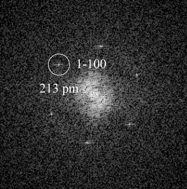
Development of high-end electron microscopes has been a vital part of the SALVE project since it was started in 2009. The SALVE I microscope was a Carl Zeiss Libra 200 - based experimental platform to evaluate the feasibility of fabricating a Cs/Cc corrected Low-Voltage HRTEM until 2011, when the construction of this microscope (SALVE II) was started at the companies Carl Zeiss and CEOS GmbH. The accelerator design and the alignment of the FEG have been optimized for low-voltage operation. For the first time this instrument can cover a voltage range from 20 to 80 kV (200 kV) without any loss in brightness (referred to the extraction voltage). At 20 kV a transfer of frequencies up to the first-order reflections in graphene could be demonstrated (Fig. 1). The benefit of imaging radiation-sensitive materials with decreased acceleration voltage was demonstrated by comparison of HRTEM dose series at 80 and 20 kV of C60 molecules encapsulated within double-walled CNTs. [1]
The prototype SALVE I microscope comprised a monochromated Libra 200 MC with in-column corrected OMEGA filter. We demonstrate that especially for low beam energies the electrostatic omega principle for monochromatization and the corrected in-column technology are beneficial for filtered images with low energy width and highly resolved spectroscopy.
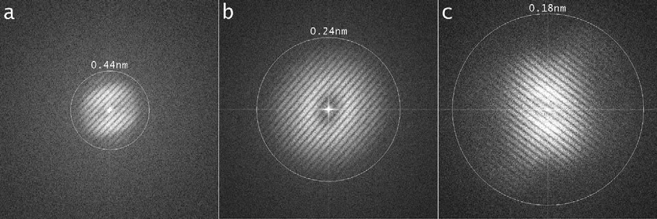
For 20 keV electrons the monochromator [2] creates high image contrast at high spatial frequencies: slit widths of 2.5 and 2 mm result in a full width at half maximum (FWHM) of 0.17 and 0.15 eV for the incident electron beam, respectively. The system received its last significant upgrade in xx/2011. This work included an imaging CEOS CS-corrector (CETCOR). The information limit of the microscope at 20 kV is determined by the combination of image spread and focus spread [3]. The focus spread limit, which comprises the effect of the chromatic aberration and other focus instabilities, can be reduced from 0.5 nm without monochromator to 0.25 nm with a reduced energy width of 0.17 eV. The image spread limit, which includes all kinds of lateral noise, has been determined to be better than 0.18 nm (Fig. 2).
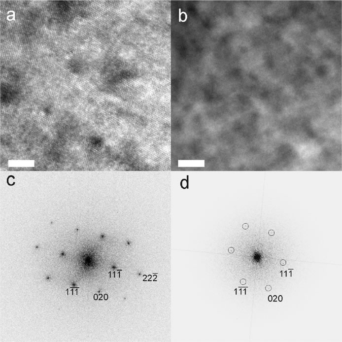
In order to judge the HRTEM imaging performance at 20 kV further, we used Si as a well-known self-supporting standard sample (Fig. 3). The influence of the monochromator on the contrast transfer is demonstrated by comparing the monochromated image (Fig. 3a) with the non-monochromated image (Fig. 3b). Clearly visible lattice fringes are only present in Fig. 3a. However, they can be seen (much weaker) in the Fourier transform of the non-monochromated image as well (Fig. 3d). The 222Si (156.7 pm) reflections can be seen as well in the Fourier transform of Fig. 3c. The high line resolution demonstrates the excellent mechanical and electrical stabilities of the system.
We used single-layer graphene as another test sample for determining the imaging properties of the microscope. Graphene produces a weak signal compared to most test samples. The lattice constant of 213 pm corresponds to a scattering angle of about 40 mrad at 20 kV (Fig. 1).
To be effective, a transmission electron microscope must keep the following critical resources in balance: the electron source, the illumination system, the imaging system, the CC/CS aberration corrector, the energy sharpness of the electron beam, the limited space in the microscope, the reduction of sample drift and the cooling capability, the electron detection efficiency, spectral recording, 3D-imaging, the possibility to conduct In-situ measurements, the vacuum system, and the environmental conditions that are necessary for the operation of a low-voltage TEM (Fig. 4).
Summary
A TEM equipped with a monochromator and the hexapole CS-corrector can be used for phase contrast imaging at 20 kV up to the limit set by the intrinsic six-fold astigmatism A5 = 15 mm. The aberration coefficients need to be tuned for a small CC-contribution to maximize the resolution. The measured values are slightly higher than the calculated values. Most probably this is due to calibration limits of magnification and tilt on which the values depend in second and fourth power, respectively.
A new CC/CS-corrector for the final SALVE II microscope which has correction tools up to axial aberrations of fourth order is feasible. Intrinsic aberrations of fifth order can by design be sufficiently small to allow for phase contrast imaging up to 50 mrad (1/0.17 nm at 20 kV).
Kaiser, U., Biskupek, J., Meyer, J. C., Leschner, J., Lechner, L., Rose, H., Stoeger-Pollach, M., Khlobystov, A. N., Hartel, P., Mueller, H., Haider, M., Eyhusen, S., & Benner, G. (2011) Transmission electron microscopy at 20kV for imaging and spectroscopy. Ultramicroscopy, 111: 1239-1246, doi: 10.1016/j.ultramic.2011.03.012
Uhlemann, S., & Haider, M. (2002) Experimental set-up of a fully electrostatic monochromator for a 200kV TEM. In The Proceedings of the 15th International Congress on Electron Microscopy, 2
Haider, M., Hartel, P., Müller, H., Uhlemann, S., & Zach, J. (2010) Information transfer in a TEM corrected for spherical and chromatic aberration. Microscopy and Microanalysis, 16: 393-408, doi: 10.1017/S1431927610013498
Schroeder, R. R., Barton, B., Rose, H. and Benner, G. (2007) Contrast Enhancement by Anamorphotic Phase Plates in an Aberration Corrected TEM. Microscopy and Microanalysis, 13: 136 – 137, doi: 10.1017/S1431927607074867
Schmidt, T., Groh, U., Fink, R., Umbach, E., Schaff, O., Engel, W., Richter, B., Kuhlenbeck, H., Schloegel, R., Freund, H.-J., Bradshaw, A. M., Preikszas, D., Hartel, P., Spehr, R., Rose, H. H., Lilienkamp, G., Bauer, E., & Benner, G. (2002) XPEEM with energy-filtering: advantages and first results from the SMART project. Surface Review and Letters, 9: 223-232, doi: 10.1142/S0218625X02001811
Rose, H. H. (1971) Properties of spherically corrected achromatic electron lenses (Spherically corrected electron lenses with improved resolving capacity and aberration compensation). Optik, 33: 1-24
Kirkland, A. I., W. O. Saxton, & G. Chand (1997) Multiple beam tilt microscopy for super resolved imaging. Journal of Electron Microscopy, 46: 11-22
Golla-Schindler, U., G. Algara-Siller, A. Orchowski, Y. Wu, T. Weil, and U. A. Kaiser (2012) First results of 20 kV EFTEM of core-shell QDS with an albumin-derived polypeptide surface coating on graphene. In EMC 2012 15th European Microscopy Congress, 16-21 September 2012, Manchester, United Kingdom
Uhlemann, S., & Haider, M. (1998) Residual wave aberrations in the first spherical aberration corrected transmission electron microscope. Ultramicroscopy, 72: 109-119, doi: 10.1016/S0304-3991(97)00102-2