Defects in bilayer silica and graphene: common trends in diverse hexagonal 2D systems
December 16, 2013 - Through a combination of aberration corrected high-resolution transmission electron microscopy (HRTEM) with density functional theory (DFT) and classical force field (CFF) calculations, an international team of scientists with the participation of the SALVE project has investigated how the symmetries of the crystal lattice determine defects and grain boundaries. These deviations from the ideal structure of a grid determine to a large extend the properties of materials. They examined two different 2D materials with hexagonal symmetry: hexagonal bilayer silica (HBS) and graphene. Their results show that the defects are largely governed by the underlying symmetry of the lattice.
For years, the family of 2-dimensional materials is continuously being expanded. One member is 2D silica: Both the tetrahedral-shaped variant covalently bonded to the substrate, and the fully saturated variant which is only weakly bound to the substrate were synthesized [1, 2, 3]. HBS has enormous technological significance, for instance as the thinnest oxide gate dielectric, as support for catalysis [4], or for the isolation of 2D materials from the substrate. Experimentally 2D silica with a different degree of disorder has been examined, from some isolated point defects over grain boundaries to complete amorphous structure [4].
Scientists of the SALVE project have worked this year on a study where the atomic rearrangements of atoms in amorphous SiO2 could be investigated experimentally for the first time [5]. After numerous previous studies with STM and AFM, in which only the surface could be examined, the successful synthesis of amorphous 2D silica [6] enabled the imaging of the atomic structure with low-voltage High Resolution Transmission Electron Microscopy (HRTEM). Now the scientists published in parallel a study on the crystalline phase of 2D silica in the journal "Scientific reports". "HBS and graphene are by far the most studied hexagonal 2D systems," said Kaiser, who conducted the experimental imaging by HRTEM. "They have very different binding properties. We wanted to analyze whether the common lattice structure results in similarities concerning the nature of defects."
As they had previously carried out already for graphene [7] and transistion metal dichalcogenides (TMD) [8], the scientists calculated the displacement threshold Td (minimum kinetic energy assigned to an atom required for it to sputter away from the system) of O and Si atoms in HBS using DFT-based molecular dynamics. The results show that only oxygen atoms are ejected at the 80 keV electron energy used for the imaging, for Si-atoms the transferred energy is generally less than the bonding energy (Fig. 1). Many topological transformations in HBS as a result of the electron beam irradiation are thus caused by an oxygen deficit of the lattice.
Point-defects
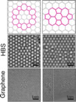
The study examines the ratio of crystalline and amorphous phases with respect to the underlying bond rotations, a method that has already been successfully applied for the analysis of sp2 carbon systems since the '90s [9]. Point defects that may be generated by one bond rotation are referred to as Stone / Wales (SW) defects (after their discoverers [9]). In graphene, the rearrangement refers to a bond between two neighbouring C atom, in HBS between four Si atoms (two in each layer) with the neighboring O atoms. Fig. 2 shows a so-called Flower-defect [10], which can be generated by 6 bond rotations and is essentially a small grain with a twist of 30° with respect to the outer grid. The defects can be observed both in graphene and in HBS. Fig. 2 also shows the butterfly-effect [11], which can be generated by removing two adjacent structural units, and then performing 2 bond rotations. One explanation why these defects can be found in both hexagonal materials was found by studying the contribution of long-range elastic fields to the formation energy. As in the case of graphene a clear minimum is observed when the defect is twisted by 30° with respect to the surrounding lattice, as in the case of the Flower defect (Fig. 3). This is because the constituent dislocations (5-7 pairs) are closely packed, leading to an efficient cancellation of elastic fields. Unlike in graphene additional relaxation of the dislocation cores exists in HBS due to the possibility of the tetrahedral formation block to rotate.
Extended topological defects
Among the extended topological defects are grain boundaries (GB). For simplification one-dimensional defects were used as an idealized model of grain boundaries, as has previously been done for graphene [12]. Deviations from the linear structure have been omitted. Furthermore, only GB structures analogous to those in graphene were included in the investigation. Direct Si-Si bonds, similar to Mo-Mo and S-S bonds observed recently in MoS2 [13] have not been taken into account. The geometry of a (1,0) GB is shown in Fig. 4. With regard to graphene [12] the calculated formation energy curves are markedly less smooth. This may be explained by the fact that in the case of HBS additional relaxation is possible as the tetrahedra can be rotated.
To determine the preferred direction of the grain boundaries DFT simulation and a model giving an analytic expression [14] were used (Fig. 5). The formation energies for graphene [12] and HBS at larger angles are significantly different: the values are significantly lower for HBS. However all investigated GB types have low formation energies by 30°, in agreement with the experimental observations for both graphene [12] as well as HBS.
Haeckelite structures
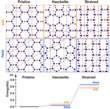
Haeckelite structures are a lattice structure, which has been theoretically proposed also for graphene [15] but never found experimentally. Nevertheless, they represent an interesting extreme case, both in terms of defect concentration, as well as in terms of stress. These structures are reminiscent of a hexagonal lattice, but are composed of 5- and 7- rings in stead of 6-membered rings. The calculated energies for HBS are higher than for the hexagonal lattice (Fig. 6) but the energy required for the production of Haeckelite structures in HBS is significantly lower than in graphene.
Similarities and differences
Although the two hexagonal systems HBS and graphene contain different atoms and have structure of varying complexity, the behavior of defects in both materials is qualitatively very similar. This applies to point-defects such as the SW defects, and extended defects such as grain boundaries. Thus, these systems differ considerably from 2D systems like TMD [13], which are multi-component systems with trigonal geometry. In these systems, the network links are more strongly constrained, so that SW transformations are much more unlikely. For example, despite experimental effort [16] SW defects have never been observed in h-BN. With regard to the fact that both, sp2-hybridized carbon and bilayer silica, can form amorphous structures and possibly Haeckelites, the result of the new study suggests that structural defects will be comparable in any hexagonal 2D system regardless of the complexity of the structural units. Such possible future systems include epitaxial atomically thin Si [17] and epitaxial transition-metal networks [18].
All conducted GB investigations show a minimum of energy of formation near 30°, which is consistent with the low energy of formation of the flower-defect and the experimental observations. The most significant difference between defects in silica and graphene is related to the formation and dynamics of defects. Due to the significantly larger number of participating atoms it is much more complex in HBS. The investigations have shown that the momentum of an electron of the electron beam is never transferred to a complete structural unit of the silica lattice, but only to a single atom within this unit. Most astonishing is that the SW transformation is still observable in silica under the electron beam. As an explanation the scientists suggest that these processes can be driven by electron irradiation through the lowering of the barriers for displacement of atoms due to vacancies from sputtered oxygen atoms and the strain that these vacancies induce.
"In the future, perhaps far more suspended hexagonal materials can be produced, which can also provide additional opportunities for study of general trends in the defect-energetic and morphology," Kaiser said.
Methods: DFT calculations were performed using the projector augmented-wave method [19] as implemented in the VASP package [20]. The classical force field (CFF) calculations were carried out using with the molecular dynamics package PARCAS [21], with a potential by Watanabe et al. [22] to describe the Si-O system.
Resource: Björkman, T., Kurasch, S., Lehtinen, O., Kotakoski, J., Yazyev, O. V., Srivastava, A., Skakalova, V., Smet, J. H., Kaiser, U. A., & Krasheninnikov, A. V. (2013). Defects in bilayer silica and graphene: common trends in diverse hexagonal two-dimensional systems. Scientific reports, 3: 3482, doi: 10.1038/srep03482, [PDF, Supporting information].
Weissenrieder, J. et al. Atomic structure of a thin silica film on a Mo (112) substrate: A two-dimensional network of SiO4 tetrahedra. (2005) Physical Review Letters, 95: 076103, doi: 10.1103/PhysRevLett.95.076103
Löffler, D. et al. (2010) Growth and structure of crystalline silica sheet on Ru(0001). Physical Review Letters, 105: 146104, doi: 10.1103/PhysRevLett.105.146104
Yang, B., Boscoboinik, J. A., Yu, X., Shaikhutdinov, S. & Freund, H.-J. Patterned defect structures predicted for graphene are observed on single-layer silica films. (2013) Nano Letters, 13: 4422–4427, doi: 10.1021/nl402264k
Shaikhutdinov, S. & Freund, H.-J. Ultrathin silica films on metals: The long and winding road to understanding the atomic structure. (2013) Advanced Materials, 25: 49–67, doi: 10.1002/adma.201203426
Huang, P. Y. et al. (2013) Imaging atomic rearrangements in two-dimensional silica glass: Watching silica’s dance. Science, 342: 224–227, doi: 10.1126/science.1242248
Huang, P. Y., Kurasch, S., Srivastava, A., Skakalova, V., Kotakoski, J., Krasheninnikov, A. V., Hovden, R., Mao, Q., Meyer, J. C., Smet, J., Muller, D. A., & Kaiser, U. A. (2012). Direct imaging of a two-dimensional silica glass on graphene. Nano letters, 12: 1081-1086, doi: 10.1021/nl204423x
Meyer, J. C. et al. (2012) An accurate measurement of electron beam induced displacement cross sections for single-layer graphene. Physical Review Letters, 108: 196102, doi: 10.1103/PhysRevLett.108.196102
Komsa, H.-P. et al. (2012) Two-dimensional transition metal dichalcogenides under electron irradiation: Defect production and doping. Physical Review Letters, 109: 035503, doi: 10.1103/PhysRevLett.109.035503
Stone, A. J., & Wales, D. J. (1986) Theoretical-studies of icosahedral C60 and some related species. Chemical Physics Letters, 128: 501–503, doi: 10.1016/0009-2614(86)80661-3
Cockayne, E. (2012) Graphing and grafting graphene: Classifying finite topological defects. Physical Review B, 85: 125409, doi: 10.1103/PhysRevB.85.125409
Zubeltzu, J., Chuvilin, A., Corsetti, F., Zurutuza, A. & Artacho, E. (2013) Knock-on damage in bilayer graphene: indications for a catalytic pathway. ArXiv e-prints, 1309.7346
Yazyev, O. V. & Louie, S. G. (2010) Topological defects in graphene: Dislocations and grain boundaries. Physical Review B, 81: 195420, doi: 10.1103/PhysRevB.81.195420
Najmaei, S. et al. (2013) Vapor phase growth and grain boundary structure of molybdenum disulphide atomic layers. Nature Materials, 12: 754–9, doi: 10.1038/nmat3673
Read, W. T. & Shockley, W. (1950) Dislocation models of crystal grain boundaries. Physical Review, 78: 275–289, doi: 10.1103/PhysRev.78.275
Appelhans, D. J., Lin, Z. & Lusk, M. T. (2010) Two-dimensional carbon semiconductor: Density functional theory calculations. Phys. Rev. B, 82: 073410, doi: 10.1103/PhysRevB.82.073410
Alem, N. et al. (2009) Atomically thin hexagonal boron nitride probed by ultrahigh resolution transmission electron microscopy. Physical Review B, 80: 155425, doi: 10.1103/PhysRevB.80.155425
Vogt, P. et al. (2012) Silicene: Compelling experimental evidence for graphene like two-dimensional silicon. Physical Review Letters, 108: 155501, doi: 10.1103/PhysRevLett.108.155501
Li, L. et al. (2013) Two-dimensional transition metal honeycomb realized: Hf on Ir(111). Nano Letters, 13: 4671–4674, doi: 10.1021/nl4019287
Blöchl, P. E. (1994) Projector augmented wave method. Physical Review B, 50: 17953, doi: 10.1103/PhysRevB.50.17953
Kresse, G. & Furthmüller, J. (1996) Efficiency of ab-initio total energy calculations for metals and semiconductors using a plane-wave basis set. Computational Materials Science, 6: 15–50, doi: 10.1016/0927-0256(96)00008-0
Nordlund, K. (1995) Molecular dynamics simulation of ion ranges in the 1–100 keV energy range. Computational Materials Science, 3: 448-456, doi: 10.1016/0927-0256(94)00085-Q
Watanabe, T., Fujiwara, H., Noguchi, H., Hoshino, T. & Ohdomari, I. (1999) Novel interatomic potential energy function for Si, O mixed systems. Japanese Journal of Applied Physics, 38: L366–L369, doi: 10.1143/JJAP.38.L366


