Atomistic Description of Electron Beam Damage in Nitrogen-Doped Graphene and Single-Walled Carbon Nanotubes.
September 24, 2012 – Although electron beam effects have been studied for decades [1], calculation of radiation damage, i.e. the interaction of the electron beam with the material under investigation is not well understood. One reason for this is that quantitative analysis of radiation damage on the atomic level became possible only recently due to the low-voltage aberration-corrected electron microscopy and the newly discovered 2D materials. Earlier this year, an experimental investigation and simulation carried out in the frame of the SALVE project provided the first accurate prediction of radiation damage for pristine graphene [2, see also this news article on the SALVE website]. It turned out that the electron irradiation-induced damage in graphene could be calculated using the displacement cross sections between the electrons and target atoms [3] when lattice vibrations were considered [2]. The simulation results were also consistent with the observation, that heating caused by the electron beam has only a negligible effect on a graphenic target material [4]. The results replaced the previous theoretical assumptions of a sharp knock-on threshold [1] and reproduced it with a smooth onset between ~80 and 110 kV, which agrees with the experimental observations [2].
In the new study, the scientists now turned towards more complex one-dimensional and two-dimensional structures. They targeted the simulation and experimental measurement of radiation damage in nitrogen-doped graphene (N-graphene) or nitrogen-doped SWCNTs (N-SWCNTs). Here the simulations were previously carried out with the tight-binding model [5], but this model predicts a displacement threshold below 14 eV for the nitrogen atom in a substitutional configuration in flat sp2-bonded carbon. The knock-on threshold should thus be below 80 kV, but aberration-corrected (AC) high-resolution TEM (HRTEM) observations have shown that N-graphene grown by chemical vapor deposition (CVD) remains stable under 80 kV conditions for long exposure times [6]. N-SWCNTs remain also stable at 80 kV [7], which contradicts the simulation result. Furthermore, EELS experiments have been typically performed with dedicated scanning TEM instruments operated at slighlty higher voltages [7, 8]. In addition, the accuracy of the experimental observation was not high enough for an accurate validation of the theoretical results.
In their new paper, the scientists now describe the successful simulation and experimental validation of the electron-beam-induced damage in these important structures by combining advanced computational methods with state-of-the-art electron microscopy. "The collaboration includes 11 authors from five European countries," recounts Toma Susi from the University of Aalto, lead author of the study. “We’d like to move towards understanding and accurately predicting radiation damage in the TEM, to find the optimum imaging conditions for every material,” says Ute Kaiser who has led the HRTEM investigation from the SALVE project.
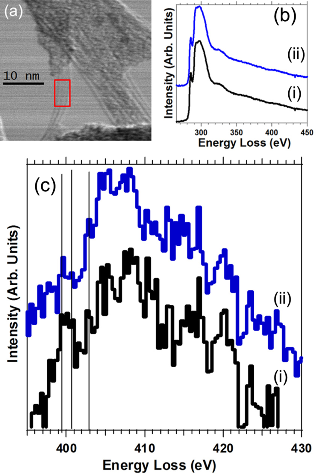
The new study showed, that ab initio molecular dynamics simulations must be carried out to correctly predict the electron irradiation stability of nitrogen-doped graphene and SWCNTs. The calculations even unraveled and explained that it is substantially easier to displace one of the carbon atoms right next to the nitrogen dopant rather than the dopant itself. Using AC-HRTEM, these events were now imaged with atomic resolution, which initially shows only nitrogen substitutions, in agreement with previous studies [6, 9-11]. In addition, consecutive EELS measurements on the same sample position[12] provided direct spectroscopic evidence for the predicted transformations.
The fact that the simulations and the experiments agree well also reveals that unlike for pristine nanotubes, knock-on damage is the main contributor in the structural damage in N-SWCNTs and N-graphene under the electron beam at 80 kV, although it is obscured by self-healing and reconstructions at room temperature (RT). This is improving the understanding of radiation damage in general.
Scientific underpinnings
Exploring radiation damage in N-graphene and N-SWNTs has gained momentum due to several factors.
- It is well-known that sp2-bonded carbon structures have exceptional physical, chemical, and electrical properties both in the case of two-dimensional graphene [13] and the cylindrical allotrope, single-walled carbon nanotube [14] (SWCNT). Doping of these structures with nitrogen is considered a viable option for realizing materials with new properties[6, 9, 15]. Significant electron doping and band gap opening has been reported for N-graphene [16]. Nitrogen doping also confers genuinely new properties, such as selective sensitivity for electrochemical catalytic activity [17].
- Overall, the latest advances, especially aberration correction, have steadily increased the importance of TEM-based methods. Cutting-edge developments in instrumentation have enabled atom-by-atom analysis of graphene [18-20] and even direct imaging of nitrogen sites [6]. For enhancing the N atom contrast, a defocus of –18 nm was used in the imaging-side aberration-corrected FEI Titan 80-300 operated at 80 kV. Electron energy loss spectra were recorded using a scanning TEM.
The simulation
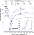
In the DFT simulation, the scientists consider an electron nucleus impact by assigning a kinetic energy to one of the atoms in the structure and then following the time evolution of the system after the impact by DFT molecular dynamics (MD) simulations. [2, 21] This allowed them to calculate the required kinetic energy TD to displace an atom from its lattice. The result for the substitutional nitrogen dopant (19.09 eV) differed considerably from the tight-binding results (<14 eV) [5]. In fact, none of the calculated TD values was below 16 eV. This discrepancy has already been observed for hexagonal BN monolayers, where the predicted using the tight-binding model [22] were found to be lower than the more accurate DFT calculations [23]. After knowing TD, the scientists could use the results obtained previously [1-3, 24] to calculate the corresponding displacement cross section (σ). The values are plotted along the TD in Figure 2 for a wide range of electron energies or, correspondingly, acceleration voltages (0 – 500 kV).
Scientists at the Universities of Vienna and Ulm were than validating the simulation results using both atomic scale LV-AC-HRTEM imaging and STEM-EELS.
HRTEM experiments
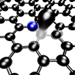
In a freestanding monolayer area of graphene (Figures 3 and 4) atomic potentials derived from all-electron DFT calculations show that electron scattering on the carbon atom next to a nitrogen differs appreciably from electron scattering on a carbon atom elsewhere in the graphene sheet. This enables to detect N substitutions in a correctly defocused TEM image because they are appearing as three darker bonds [6].
By comparing the HRTEM images with DFT simulation, structural changes can now be followed on the atomic scale and the transformation of the substitutional configuration, where one nitrogen atom substitutes on carbon atom of the graphene lattice could be observed. Using the earlier model [5], one should expect a cross section of more than 2 barn for displacing one such nitrogen dopant, already considering lattice vibrations [2] under our 80 kV imaging conditions. Such a high cross section was not observed. By contrast, none of the N atoms was sputtered by the end of the experiments. In contrast, the scientists observed another change in the atomic structure of the dopant sites during imaging. From Figure 3, it can be clearly seen that, instead of the dopant atom, the first atom displaced by the electron beam is one of the three carbon atoms next to it. The statistical estimate for the upper limit of the displacement cross section of the ejected carbon atoms is 0.16 barn, which can be directly compared with the calculation result of about 0.03 barn (Figure 2). Considering the inaccuracies resulting from experimental uncertainties as well as the sensitivity of the theoretical cross section calculations at small values, this can be considered a good agreement. Another point to consider is that, due to the high computational cost of dynamical DFT simulations, the scientists could only calculate displacements in the direction perpendicular to the graphene plane. This may also contribute to the discrepancy since non-orthogonal displacements of atoms with neighbors of different mass may have lower thresholds, unlike atoms in pristine graphene [30]. In addition, defect healing via adatom migration in the experiments can be considered to have a significant impact on the radiation damage.
The effect of curvature
The present computational power did not allow to extend the simulations to curved structures. Fortunately, the effects of curvature of the structure [5, 30, 31] as well as the displacement direction [4, 22, 30] are relatively well-understood based on previous studies. The effect of curvature starts to be significant at d ~ 2 nm and TD decreases with increased curvature for smaller nanotubes (Figure 5). Atoms in the “sides” of nanotubes (with respect to the electron beam) are known to have much larger thresholds [4]. The displacements of the atoms located at the “top” and “bottom” of the tube should dominate the apparent σ in SWCNT experiments.
Considering the curvature effect in N-SWCNTs, the scientists have used an empirical function to describe the diameter dependency of TD using literature data [5, 30, 31] (Figure 5). Employing this function, they estimate the expected thresholds for nanotubes with different diameters from values calculated for graphene. The values for the dopant configurations are presented in Figure 2 as well as for single and double vacancies in un-doped structures. They also presented the calculated σ for each configuration to facilitate the comparison with experiments presented below.
An innovative model helped to bridge between the simulation and the experimental observation of the radiation damage in N-SWCNTs. They measured the relative diameter reduction as a function of the irradiation dose, which includes contributions from all processes (e.g., knock-on damage, healing, and reconstruction). In Figure 6, the diameters of three nanotubes with different initial sizes (2.2, 1.8, and 1.4 nm) is shown as a function of the irradiation dose. The corresponding apparent cross sections obtained from these data are 0.2, 0.5, and 1.1 barn, respectively. The decreasing TD (and correspondingly increasing σ;) with decreasing diameter, as shown in Figure 5 could in that way be validated experimentally. Even, the values themselves were in the expected range.
What present models can - and can't
"We have now shown, that also for more complex structures it is possible to model the knock-on threshold of flat structures using the presently available DFT calculations. When curved structures are considered and when electron-electron interactions are important, the required computational power is still higher than what is presently available. We demonstrated that at 80 kV, radiation damage is mainly knock-on damage. At lower accelerating voltages below the knock-on threshold, radiation damage will be determined by electron-electron interaction and new models will have to be applied.", says Ute Kaiser, director of the SALVE project. “The collaboration within this project demonstrated, how the cutting-edge technology in simulation and experiments contribute to the advancement of our understanding of the interaction of electrons and matter. The increasing resolution of the electron microscope has significantly contributed to provide atomically resolved data in the last 5 years and the extensions of the voltage range where atomic resolution is available will hopefully contribute with even more comprehensive data in the future.”
Highlighted Topics
Resource: Susi, T., Kotakoski, J., Arenal, R., Kurasch, S., Jiang, H., Skakalova, V., Stephan, O., Krasheninnikov, A. V., Kaupinen, E. I., Kaiser, U. A., & Meyer, J. C. (2012). Atomistic description of electron beam damage in nitrogen-doped graphene and single-walled carbon nanotubes. ACS nano, 6, 8837-8846., doi: 10.1021/nn303944f, [PDF].
Banhart, F. (1999). Irradiation effects in carbon nanostructures. Reports on Progress in Physics, 62(8), 1181.
Meyer, J. C., Eder, F., Kurasch, S., Skakalova, V., Kotakoski, J., Park, H. J., Roth, S., Chuvilin, A., Eyhusen, S., Benner, G., Krasheninnikov, A. V., & Kaiser, U. (2012). Accurate measurement of electron beam induced displacement cross sections for single-layer graphene. Physical Review Letters, 108(19), 196102.
McKinley Jr, W. A., & Feshbach, H. (1948). The coulomb scattering of relativistic electrons by nuclei. Physical Review, 74(12), 1759.
Zobelli, A., Gloter, A., Ewels, C. P., & Colliex, C. (2008). Shaping single walled nanotubes with an electron beam. Physical Review B, 77(4), 045410.
Loponen, T., Krasheninnikov, A. V., Kaukonen, M., & Nieminen, R. M. (2006). Nitrogen-doped carbon nanotubes under electron irradiation simulated with a tight-binding model. Physical Review B, 74(7), 073409.
Meyer, J. C., Kurasch, S., Park, H. J., Skakalova, V., Künzel, D., Groß, A., Chuvilin, A., Algara-Siller, G., Roth, S., Iwasaki, T., Starke, U., Smet, J. H., & Kaiser, U. (2011). Experimental analysis of charge redistribution due to chemical bonding by high-resolution transmission electron microscopy. Nature Materials, 10(3), 209-215.
Susi, T., Kaskela, A., Zhu, Z., Ayala, P., Arenal, R., Tian, Y., Laiho, P., Mali, J., Nasibulin, A. G., Jiang, H., Lanzani, G., Stephan, O., Laasonen, K., Pichler, T., Loiseau, A., & Kauppinen, E. I. (2011). Nitrogen-doped single-walled carbon nanotube thin films exhibiting anomalous sheet resistances. Chemistry of Materials, 23(8), 2201-2208.
Panchakarla, L. S., Subrahmanyam, K. S., Saha, S. K., Govindaraj, A., Krishnamurthy, H. R., Waghmare, U. V., & Rao, C. N. R. (2009). Synthesis, structure and properties of boron and nitrogen doped graphene. Advanced Materials, 21(46), 4726-4730.
Wei, D., Liu, Y., Wang, Y., Zhang, H., Huang, L., & Yu, G. (2009). Synthesis of N-doped graphene by chemical vapor deposition and its electrical properties. Nano Letters, 9(5), 1752-1758.
Zhao, L., He, R., Rim, K. T., Schiros, T., Kim, K. S., Zhou, H., Gutiérrez, C., Chockalingam, S. P., Arguello, C. J., Pálová, L., Nordlund, D., Hybertsen, M. S., Reichmann, D. R., Heinz, T. F., Kim, P., Pinczuk, A., Flynn, G. W., & Pasupathy, A. N. (2011). Visualizing individual nitrogen dopants in monolayer graphene. Science, 333(6045), 999-1003.
Fujimoto, Y., & Saito, S. (2011). Formation, stabilities, and electronic properties of nitrogen defects in graphene. Physical Review B, 84(24), 245446.
Colliex, C. (1996). New trends in STEM-based nano-EELS analysis. Journal of Electron Microscopy, 45(1), 44-50.
Geim, A. K., & Novoselov, K. S. (2007). The rise of graphene. Nature Materials, 6(3), 183-191.
Smalley, R. E. (2003). Carbon nanotubes: synthesis, structure, properties, and applications (Vol. 80). M. S. Dresselhaus, G. Dresselhaus, & P. Avouris (Eds.). Springer Science & Business Media.
Arenal, R., Blase, X., & Loiseau, A. (2010). Boron-nitride and boron-carbonitride nanotubes: synthesis, characterization and theory. Advances in Physics, 59(2), 101-179.
Usachov, D., Vilkov, O., Gruneis, A., Haberer, D., Fedorov, A., Adamchuk, V. K., Preobrajenski, A. B., Dudin, P., Barinov, A., Oehzelt, M., Laubschat, C., & Vialikh, D. V. (2011). Nitrogen-doped graphene: efficient growth, structure, and electronic properties. Nano Letters, 11(12), 5401-5407.
Gong, K., Du, F., Xia, Z., Durstock, M., & Dai, L. (2009). Nitrogen-doped carbon nanotube arrays with high electrocatalytic activity for oxygen reduction. Science, 323(5915), 760-764.
Suenaga, K., & Koshino, M. (2010). Atom-by-atom spectroscopy at graphene edge. Nature, 468(7327), 1088-1090.
Krivanek, O. L., Chisholm, M. F., Nicolosi, V., Pennycook, T. J., Corbin, G. J., Dellby, N., Murfitt, M. F., Own, C. S., Szilagyi, Z. S., Oxley, M. P., Pantelides, S. T., & Pennycook, S. J. (2010). Atom-by-atom structural and chemical analysis by annular dark-field electron microscopy. Nature, 464(7288), 571-574.
Kurasch, S., Kotakoski, J., Lehtinen, O., Skákalová, V., Smet, J., Krill III, C. E., Krasheninnikov, A. V., & Kaiser, U. (2012). Atom-by-atom observation of grain boundary migration in graphene. Nano Letters, 12(6), 3168-3173.
Kotakoski, J., Santos-Cottin, D., & Krasheninnikov, A. V. (2011). Stability of graphene edges under electron beam: equilibrium energetics versus dynamic effects. ACS Nano, 6(1), 671-676.
Zobelli, A., Gloter, A., Ewels, C. P., Seifert, G., & Colliex, C. (2007). Electron knock-on cross section of carbon and boron nitride nanotubes. Physical Review B, 75(24), 245402.
Kotakoski, J., Jin, C. H., Lehtinen, O., Suenaga, K., & Krasheninnikov, A. V. (2010). Electron knock-on damage in hexagonal boron nitride monolayers. Physical Review B, 82(11), 113404.
Tewary, V. K., & Yang, B. (2009). Singular behavior of the Debye-Waller factor of graphene. Physical Review B, 79(12), 125416.
Ewels, C. P., & Glerup, M. (2005). Nitrogen doping in carbon nanotubes. Journal of Nanoscience and Nanotechnology, 5(9), 1345-1363.
Ayala, P., Arenal, R., Loiseau, A., Rubio, A., & Pichler, T. (2010). The physical and chemical properties of heteronanotubes. Reviews of Modern Physics, 82(2), 1843.
Rocha, A. R., Rossi, M., da Silva, A. J., & Fazzio, A. (2010). Realistic calculations of carbon-based disordered systems. Journal of Physics D: Applied Physics, 43(37), 374002.
Cho, Y. J., Kim, H. S., Baik, S. Y., Myung, Y., Jung, C. S., Kim, C. H., Park, J., & Kang, H. S. (2011). Selective nitrogen-doping structure of nanosize graphitic layers. The Journal of Physical Chemistry C, 115(9), 3737-3744.
Kurasch, S., Meyer, J. C., Künzel, D., Groß, A., & Kaiser, U. (2011). Simulation of bonding effects in HRTEM images of light element materials. Beilstein Journal of Nanotechnology, 2(1), 394-404.
Kotakoski, J., Meyer, J. C., Kurasch, S., Santos-Cottin, D., Kaiser, U., & Krasheninnikov, A. V. (2011). Stone-Wales-type transformations in carbon nanostructures driven by electron irradiation. Physical Review B, 83(24), 245420.
Banhart, F., Li, J. X., & Krasheninnikov, A. V. (2005). Carbon nanotubes under electron irradiation: stability of the tubes and their action as pipes for atom transport. Physical Review B, 71(24), 241408.
Krasheninnikov, A. V., Banhart, F., Li, J. X., Foster, A. S., & Nieminen, R. M. (2005). Stability of carbon nanotubes under electron irradiation: role of tube diameter and chirality. Physical Review B, 72(12), 125428.
Elias, A. L., Ayala, P., Zamudio, A., Grobosch, M., Cruz-Silva, E., Romo-Herrera, J. M., Campos-Delgado, J., Terrones, H., & Pichler, T., Terrones, M. (2010). Spectroscopic characterization of N-doped single-walled carbon nanotube strands: An x-ray photoelectron spectroscopy and Raman study. Journal of Nanoscience and Nanotechnology, 10(6), 3959-3964.
Glerup, M., Steinmetz, J., Samaille, D., Stephan, O., Enouz, S., Loiseau, A., Roth, S., & Bernier, P. (2004). Synthesis of N-doped SWNT using the arc-discharge procedure. Chemical Physics Letters, 387(1), 193-197.
Susi, T., Zhu, Z., Ruiz‐Soria, G., Arenal, R., Ayala, P., Nasibulin, A. G., Lin, H., Jiang, H., Stepahn, O., Pichler, T., Loiseau, A., & Kauppinen, E. I. (2010). Nitrogen‐doped SWCNT synthesis using ammonia and carbon monoxide. physica status solidi (b), 247(11‐12), 2726-2729.
Arenal, R., De la Pena, F., Stephan, O., Walls, M., Tence, M., Loiseau, A., & Colliex, C. (2008). Extending the analysis of EELS spectrum-imaging data, from elemental to bond mapping in complex nanostructures. Ultramicroscopy, 109(1), 32-38.
Pels, J. R., Kapteijn, F., Moulijn, J. A., Zhu, Q., & Thomas, K. M. (1995). Evolution of nitrogen functionalities in carbonaceous materials during pyrolysis. Carbon, 33(11), 1641-1653.


