Atom migration in MoTe2
June 14, 2021 - Tailoring the local optical and electronic properties of 2D TMDs is a long standing challenge in materials science. Two research groups at the University of Ulm, the Helmholtz-Center Dresden-Rossendorf in Germany and the University of Aalto in Finland have published new findings on atom migrations in single-layer 1H-MoTe2 in the transmission electron microscope at an electron energy of 40 keV, which should facilitate tailoring the local properties of the material.
Low-voltage aberration-corrected transmission electron microscopy (LV-AC-TEM) in combination with density functional theory (DFT) was performed to study open questions regarding the dynamics of extended defects in a two-dimensional (2D) transition metal dichalcogenide (TMDs) bringing together two groups of theoretical and experimental researchers from Germany and Finland. Based on atomic-resolution data measured with the Cc-Cs corrected SALVE microscope observed and modeled the in situ formation of atomic defects and their dynamics in 1H-MoTe2 and also analyzed whether it is possible to induce these transformations in a controllable manner using electron irradiation in the TEM at a very low accelerating voltage of 40 kV.
“Understanding the transformations of 2D materials under an electron beam may potentially open new pathways for defect-based engineering of devices such as single-photon emitters, quantum dots, and metallic vacancy lines embedded into semiconducting 2D material,” said the authors. “We were able to follow the migration of atoms on the atomic scale and to understand the migration and agglomeration of single Te vacancies with the help of supporting DFT calculations.”
2D TMDs can exist in different phases, as trigonal prismatic (H), octahedral (T), or monoclinic (T′) phase structures. (1, 2) 1H-TMDs have a hexagonal lattice with alternating metal and chalcogen atom columns, wherein the two chalcogen atoms are on top of each other. In the 1T-TMD phase, the chalcogen atoms of the first chalcogenide layer are located in the center of the hexagonal rings of the second layer. However, in group-VI chalcogenides, this phase should transform to the lower-energy distorted 1T′-phase. (1) Transformations from 1H to the 1T′-phase can be induced using several approaches, for example, by electrostatic doping or atomic defect creation. (3)
Molybdenum ditelluride (MoTe2) is one of the most interesting 2D TMDs as the energy difference between the semiconducting 1H and the metallic 1T′-phase is only ∼31 meV per unit cell; (4) therefore, a phase transformation can easily be induced by heating, (5) electrostatic gating, (6) doping, (7) or adsorption of atoms. (8) Using atomistic simulations, Duerloo et al. (4) predicted that mechanical deformations can cause a switch between the semiconducting and the metallic phase in single-layer TMDs such as MoTe2. Uniaxial tensile strains along the b axis (armchair direction) ranging from 0.3 to 3% should transform MoTe2 from the 1H to the 1T′-phase already at room temperature. (4)
Crystalline imperfections, such as vacancies, in 2D MoTe2 can induce a phase transformation between the 1H and 1T′ phases. (6) A substantial amount of knowledge on the behavior of intrinsic and extrinsic defects, such as vacancies or impurities, has been obtained. (9, 10) Many insights came from the high-resolution transmission electron microscopy (HRTEM) experiments, which allow “seeing” every atom in the 2D system and following defect structure evolution in real time. Defects can deliberately be produced by the electron beam. In particular, the investigations for single-layer MoTe2 showed that point defects induced in one chalcogenide layer agglomerate mainly into single vacancy lines, whereas defects in both chalcogen layers are predominantly forming extended defects. (10) Defect-mediated transformations from the 1H into the 1T′ phase, the formation of inversion domains with mirror twin boundaries, and complicated extended defects, which can be referred to as quantum dots, have been observed under electron irradiation. (10)
In their new study, which can be referred to as a follow-up work of a previous paper (10), the authors addressed the open issue: (i) how do extended defects migrate and what elementary migration events are responsible for sliding and rotating single vacancy lines, forming inversion domains, and local transformations to the 1T′-phase? (ii) How do external factors such as strain govern the evolution of complex defects? (iii) What are the energy barriers for these processes? (iv) Is it possible to induce these transformations in a controllable manner using electron irradiation in the TEM?
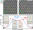
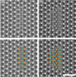
To establish a link to the previously published HRTEM data on the behavior of isolated point defects in MoTe2 (10) and their study of multiple vacancy defects, the authors analyzed the defect diffusion by considering the migration of vacancies and their agglomeration into extended defects. Figures 1-5 show Cc/Cs-corrected 40 kV HRTEM images of freestanding 1H-MoTe2. The honeycomb structure in Figure 1a,b is constructed by Mo atoms (indicated by turquoise dots in the bottom left) and brighter Te2 columns (indicated by orange dots). Red arrows mark a single vacancy (V1Te). Orange arrows describe the movement of an atom through the lattice and the shift of Te2 columns are indicated by the black arrows. The authors analyzed the migration of dislocations, starting from a single vacancy to the migration of longer vacancy lines through the lattice.
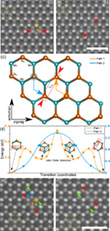
The DFT calculations that the authors performed sheded more light on the detailed paths of the transformations. For a rotation of a V4Te line, their DFT calculations resulted in two different possible migration processes. First, the rotation can be achieved by a step-by-step execution event. Or, second, all involved atoms move into a hexagonal center in the structure so that a triangular 1T-phase is formed (cf. inset in Figure 3g), from which the atoms can reorient themselves and rotate the vacancy line. The energy pathways for the two exemplified migration processes are shown in Figure 3g. While the triangular 1T-phase has low energy, the migration barriers to that configuration are much higher than for the path-1 events. The rotation occurs very fast, and no fully developed triangular intermediate state (as shown in Figure 3g, middle inset), where the tellurium atoms are located in the center of the hexagons, could be imaged experimentally. This supports the notion that the rotation process proceeds via sequential events. The results indicate that these events occur very fast, one after another, but after most of the attempts, the system returns to the original vacancy line configuration.
To understand the driving force for the observed transformations, the authors then investigated the development of strain around line defects and the effect of the transformations may strongly depend on the origin of the strin in the 2D materials and their heterostructures. (15) It was already known that there is a fundamental difference between the “standard” approach where strain is created externally, by using, for example, an atom force microscope (AFM) cantilever or deposition on elastomeric substrates (16) and the situation in an electron microscope, where strain naturally comes from the point and line defects created by the electron beam. To understand the transformations, the scientists analayzed strain of line defects and tensile strain. In total, the larger the occurring strain in the uniaxial-y direction, the more energetically favorable the rotation becomes.
To understand the energetics of the phase transformation in more detail, the authors then analyzed between the formation energies on the example of the 1T′-phasevacancy line (cf. Figure 7a). The results in Figure 7b suggest that the formation energy per missing Te atom for single vacancy lines is lower than for the trapezoidal 1T′-phase although the difference in the formation energies per Te atom between the single vacancy line and the local 1T′-phase gets smaller with the increasing length of the vacancy line. As the transformation effect has been observed more often in longer line defects, these experimental results were confirmed by the DFT calculations of the scientists.
Although single Te vacancy lines are formed under the electron beam and should be energetically more stable than the trapezoidal 1T′-phase island, the transformation was often observed, and the structure was remarkably stable under irradiation with energetic electrons. The authors that some of the phases, such as the 1T′-phase, may be stabilized by strain. The calculated lattice constants are a = b = 3.54 Å for the 1H-phase and a = 3.48 Å and b = 7.23 Å for the 1T′-phase. Embedding a 1T′-phase region within an unstrained 1H-phase matrix thus means that the 1T′-phase region is tensile strained along a and compressively strained along b.
In the literature, some the scientists had previously chosen the hybrid Hartree–Fock/DFT method with the Heyd–Scuseria–Ernzerhof functional (4) as an exchange–correlation functional. This functional gave lower stress values than the PBE/DFT approach that the authors had used in their new study to interpret their atomically resolved AC-HRTEM data. Furthermore, impurities and entropic contributions to the free energy at finite temperatures can also play an important role, facilitating the transition to the T′-phase. (17) The previosu simulations (4) had indicated that other components of strain and finite temperatures substantially reduce the critical strain value. While we know that vacancies induce tensile strain, a precise value is difficult to estimate.
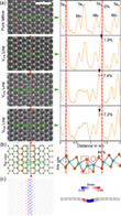
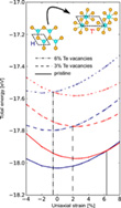
The new data the authors presented now, see Figure 8, clearly indicated that the introduction of Te vacancies lowers the required strain for a phase transformation in 1H-MoTe2. Based on these results and assuming that the migration barriers shown in Figure 3g are not dramatically increased by the presence of small tensile strain, the most probable explanation is that the strain and the presence of Te vacancies result in a phase transformation that is further facilitated by electron beam-induced bond breaking at a very low acceleratiing voltage of only 40 keV.
In summary, the authors had addressed many open questions related to the transformation pathways to complex defect structures such as single Te vacancy lines and small islands of the 1T′-phase. Their experimental data combined with the results of DFT calculations revealed that (i) all migrations of vacancies and extended defect structures can be deconstructed to two paths of motion of single Te atoms through the hexagonal crystal lattice. This step-by-step process leads to an even lower energy barrier for the movement of single Te vacancy lines than for individual single Te vacancies. The observed elementary migration events of the defect structures are likely further accelerated by the energy transfer from the electron beam. (ii) The apparent changes in the preferred orientation of the line defects and stability of 1T′-phase regions are related to the development of strain in the sample, induced by the formation of vacancies that are the atoms sputtered by the electron beam.
From the new results it became evident how energetic electrons provide the possibility to create defects and modify their density and in general their arrangement in atomically thin MoTe2. The new findings should enhance the control over defects. "Mechanical strain can come not only from the defects but also be created externally. A synergetic can be experimentally achieved by combining TEM with a scanning tunneling microscope (STM) or an atom force microscope (AFM) located inside the TEM chamber", Ute Kaiser who led the TEM studies at the University of Ulm said. On a large scale (but without in situ control of defects), defects can be produced by ion irradiation (18) and then strain can be applied by bending the substrate (16) or using AFM. (19) The understanding of defect dynamics in 2D transition metal dichalcogenides should facilitate tailoring their local optical and electronic properties.
Resource: Janis Köster, Mahdi Ghorbani-Asl, Hannu-Pekka Komsa, Tibor Lehnert, Silvan Kretschmer, Arkady V Krasheninnikov, Ute Kaiser. Defect Agglomeration and Electron-Beam-Induced Local-Phase Transformations in Single-Layer MoTe2 (2021) The Journal of Physical Chemistry C 125, 13601-13609, doi: 10.1021/acs.jpcc.1c02202, [PDF].
-
Chhowalla, M.; Shin, H. S.; Eda, G.; Li, L. J.; Loh, K. P.; Zhang, H. The chemistry of two-dimensional layered transition metal dichalcogenide nanosheets. Nat. Chem. 2013, 5, 263– 275.
-
Pizzochero, M.; Yazyev, O. V. Point defects in the 1T′ and 2H phases of single-layer MoS2: A comparative first-principles study. Phys. Rev. B 2017, 96, 245402.
-
Lehnert, T.; Lehtinen, O.; Algara-Siller, G.; Kaiser, U. Electron radiation damage mechanisms in 2D MoSe2. Appl. Phys. Lett. 2017, 110, 033106.
-
Duerloo, K.-A. N.; Li, Y.; Reed, E. J. Structural phase transitions in two-dimensional Mo- and W-dichalcogenide monolayers. Nat. Commun. 2014, 5, 4214.
-
Brown, B. E. The crystal structures of WTe2 and high-temperature MoTe2. Acta Crystallogr. 1966, 20, 268– 274.
-
Cho, S.; Kim, S.; Kim, J. H.; Zhao, J.; Seok, J.; Keum, D. H.; Baik, J.; Choe, D.-H.; Chang, K. J.; Suenaga, K. Phase patterning for ohmic homojunction contact in MoTe2. Science 2015, 349, 625– 628.
-
Wang, Y.; Xiao, J.; Zhu, H.; Li, Y.; Alsaid, Y.; Fong, K. Y.; Zhou, Y.; Wang, S.; Shi, W.; Wang, Y. Structural phase transition in monolayer MoTe2 driven by electrostatic doping. Nature 2017, 550, 487– 491.
-
Zhou, Y.; Reed, E. J. Structural phase stability control of monolayer MoTe2 with adsorbed atoms and molecules. J. Phys. Chem. C 2015, 119, 21674– 21680.
-
Komsa, H. P.; Kotakoski, J.; Kurasch, S.; Lehtinen, O.; Kaiser, U.; Krasheninnikov, A. V. Two-dimensional transition metal dichalcogenides under electron irradiation: Defect production and doping. Phys. Rev. Lett. 2012, 109, 035503.
-
Lehnert, T.; Ghorbani-Asl, M.; Köster, J.; Lee, Z.; Krasheninnikov, A. V.; Kaiser, U. Electron-beam-driven structure evolution of single-layer MoTe2 for quantum devices. ACS Appl. Nano Mater. 2019, 2, 3262– 3270.
-
Komsa, H.-P.; Kurasch, S.; Lehtinen, O.; Kaiser, U.; Krasheninnikov, A. V. From point to extended defects in two-dimensional MoS2: Evolution of atomic structure under electron irradiation. Phys. Rev. B: Condens. Matter Mater. Phys. 2013, 88, 035301.
-
Lee, C.-W.; Schleife, A. Hot-electron-mediated Ion diffusion in semiconductors for ion-beam nanostructuring. Nano Lett. 2019, 19, 3939– 3947.
-
Kretschmer, S.; Lehnert, T.; Kaiser, U.; Krasheninnikov, A. V. Formation of defects in two-dimensional MoS2 in the transmission electron microscope at electron energies below the knock-on threshold: the role of electronic excitations. Nano Lett. 2020, 20, 2865– 2870.
-
Sensoy, M. G.; Vinichenko, D.; Chen, W.; Friend, C. M.; Kaxiras, E. Strain effects on the behavior of isolated and paired sulfur vacancy defects in monolayer MoS2. Phys. Rev. B 2017, 95, 014106.
-
Novoselov, K. S.; Castro Neto, A. H. Two-dimensional crystals-based heterostructures: materials with tailored properties. Phys. Scr. 2012, 2012, 014006.
-
Castellanos-Gomez, A.; Roldán, R.; Cappelluti, E.; Buscema, M.; Guinea, F.; van der Zant, H. S. J.; Steele, G. A. Local strain engineering in atomically thin MoS2. Nano Lett. 2013, 13, 5361– 5366.
-
Kretschmer, S.; Komsa, H.-P.; Bøggild, P.; Krasheninnikov, A. V. Structural transformations in two-dimensional transition-metal dichalcogenide MoS2 under an electron beam: insights from first-principles calculations. J. Phys. Chem. Lett. 2017, 8, 3061– 3067.
-
Iberi, V.; Liang, L.; Ievlev, A. V.; Stanford, M. G.; Lin, M.-W.; Li, X.; Mahjouri-Samani, M.; Jesse, S.; Sumpter, B. G.; Kalinin, S. V. Nanoforging single layer MoSe2 through defect engineering with focused helium ion beams. Sci. Rep. 2016, 6, 30481.
-
Manzeli, S.; Allain, A.; Ghadimi, A.; Kis, A. Piezoresistivity and strain-induced band gap tuning in atomically thin MoS2. Nano Lett. 2015, 15, 5330– 5335.

