Bottom-up synthesis of nanoporous graphene
May 22, 2019 - Scientists from Germany announced today that they have synthesized new self-assembled monolayers (SAMs) that, after electron irradiation and pyrolysis on copper, can be transformed into CNM with graphene islands or nanoporous graphene. Combined dark-field TEM, AC-HRTEM and electron diffraction data confirmed the crystallinity and porosity of the composite material in agreement with a detailed crystallization model.
Since it was revealed that the covalent functionalization of the graphene plane leads to defects and deterioration of electronic properties,[1] nanoporous graphene is attractive for numerous applications.[2-5] For instance, graphene nanomeshes[6] with high electronic quality and numerous edges available for functionalization are an interesting alternative for sensor applications with functionalized graphene.[1,6,7] Moreover, focused ion beam milling with gallium or helium ions was used to produce nanopores in graphene, which are also of interest for ultrafiltration or in battery research.[2]
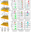
Scientists have now shown an alternative manufacturing method for nanoporous graphene, shown schematically in Figure 1a,b. Aromatic self-assembled monolayers (SAMs) are used as molecular precursors. In the first step, the monolayers are produced by vacuum vapor deposition on copper substrate. In the second step, Figure 1a (ii), the SAM is converted into a carbon nanomembrane (CNM) by low-energy electron irradiation.[8,9] Different CNMs from various precursor molecules(PTP, DPTP and TPP) have been synthesized to adjust the properties of the CNM and their structure.[10, 11] Vacuum pyrolysis is finally employed to form graphene islands in the CNM in step (iii).[12] It had been shown before that pyrolysis of CNMs on catalytic materials can lead to crystallization and formation of graphene islands in a CNM,[13] but for the first time, the scientists used SAMs made from special nitrogen-containing molecules, which enabled additional nanopores to be formed during pyrolysis by extrusion of the nitrogen atoms and finally enabled the formation of highly crystalline nanoporous graphene (Figure 1a (iv)).
To precisely characterize the pyrolized CNM sheets, the scientists used a wide range of surface science and electrical characterization techniques. Here shown by X-ray photoelectron spectroscopy (XPS), Raman spectroscopy, aberration-corrected transmission electron microscopy (AC-TEM) and characterization of electrical devices.
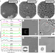
As can be seen from the XPS and Raman spectra as well as from the TEM data (see Figure 1c-e and 2d), annealing the PTP and DPTP samples at higher temperatures leads to their conversion into nanoporous graphene with higher crystallinity and simultaneously to the desorption of nitrogen. In the case of the DPTP-CNMs, which have a lower surface density than the PTP-CNMs, the transformation into nanoporous graphene accurs at an about 10 K lower temperature. For temperatures of ~ 950–980 K, the respective N1s XPS data shows, for PTP and DPTP-CNMs, the presence of two nitrogen species: one with a BE of 400.7 eV (blue), which can be attributed to pyrrole or tertiary nitrogen[14] and another at a BE of 401.6-402 eV (green) due to the formation of graphitic nitrogen. For TPP CNMs, the scientists found several cases where individually nitrogen atoms were incorporated into the graphene lattice without any noticeable nanopore formation (Figure 2f), as reported in a recent PhD thesis from one of the Co-authors.[15] The increasing ratio of sp2 bonded carbon shows the formation of graphene islands in the CNM, which is further confirmed by the respective Raman spectra and TEM data in Figure 2d. The presence of nanopores in the carbon-based nanostructures formed by pyrolysis of the PTP and DPTP-CNMs is also clearly demonstrated by dark field TEM (DF-TEM) (see Figure 2a-c).
Charge Carrier Transport in the nanostructures.
In addition to the surface characterization, the scientists used the material for fabricating FET devices. Here it was possible to measure the electronic conductivity and the mobility of the charge carriers in the layers that are partially converted to graphene sheets in detail (Figure 3). The specific resistance varied between very high resistive samples (> 108 kΩ/sq) and around 100 kΩ/sq for samples with low and high pyrolysis temperatures (Tp ≈ 950–1050 K). It was unclear, for example, what caused the wide range of electrical conductivities observed in the material and how they are related to the observed Raman spectra.
The scientists could approach the solution of this problem, as it became clear that for a sample with high electrical resistance the variable range hopping (VRH) model could be successfully employed to describe the experimental data (Figure 3a).[12] Furthermore, the transport in samples with a higher crystallinity was well described with the typical transfer characteristic for single-layer graphene sheets. (Figure 3b) ρ(Tp) correlates well with the structural and chemical changes observed during pyrolysis by Raman spectroscopy, HRTEM and XPS (Figures 1,2). Taking the experimentally determined porosity values into account, a mobility of up to 600 cm2/(Vs) was found experimentally.
The electrical measurement data indicated further that the transport regime was electrical percolation. By means of the electrical measurements, the scientists were thus able to conclude that, depending on the pyrolysis temperature, graphene areas of different sizes are formed in a CNM matrix, which finally merge at the threshold temperature. These areas were also observed in the HRTEM study (see Figure 4a). "We were for the first time able to clearly identify the crystals in the TEM," said Ute Kaiser. After earlier reports on crystalline areas in pyrolyzed CNMs by atomically resolved scanning tunneling microscopy (STM),[13] these areas could now be imaged using the Cc/Cs corrected SALVE TEM.
An analysis of the conductivity as a function of the crystallinity is shown in Figure 3c. To measure the crystallinity of the sample, the scientists used the XPS data. The model describes the experimental data very well over a wide range of conductivitties over 8 orders of magnitude.
The XPS, Raman spectroscopy, HRTEM, and electrical transport data show that (i) CNMs are converted to thermally converted graphene sheets at temperatures above 950 K, (ii) only a certain part for a given pyrolysis temperature the CNM is converted (iii) the conversion is complete within a relatively short time < 1 h; and (iv) island growth of graphene occurs.
Kinetic Model Description of the Conversion of CNMs into Graphene via Pyrolysis
Why the new material can have a wide range of crystal and pore sizes was revealed with numerical calculations. The scientists compared the experimental data with various models. A good match was found for one describing the crystallization behavior of a molecular, covalently bound material.[16] The crystallization front hinders the growth of the crystalline phase, leading to an asymptotic crystallinity <1 below a threshold pyrolysis temperature (Figure 4). Crystalline graphene areas fill the entire layer above the threshold temperature.
The crystallinity, which resulted from the growth parameters of the crystallization model (Figure 4c). At 1043 K, a crystallinity very close to 1 was achieved. This is in good agreement with the Raman showing the characteristic bands of graphene.
In the new material, the size of the graphene islands formed can also be adjusted either through the pyrolysis temperature or possibly also the pyrolysis time. Such composites can exhibit a variety of useful functional properties for catalytic and photonic applications.
Resource: Christof Neumann, David Kaiser, Michael J. Mohn, Matthias Füser, Nils-Eike Weber, Oliver Reimer, Armin Gölzhäuser, Thomas Weimann, Andreas Terfort, Ute Kaiser, and Andrey Turchanin (2019) Bottom-Up Synthesis of Graphene Monolayers with Tunable Crystallinity and Porosity. ACS Nano, 13, 7310-7322, doi: 10.1021/acsnano.9b03475.
-
Georgakilas, V.; Otyepka, M.; Bourlinos, A. B.; Chandra, V.; Kim, N.; Kemp, K. C.; Hobza, P.; Zboril, R.; Kim, K. S. Functionalization of graphene: Covalent and non-covalent approaches, derivatives and applications. Chem. Rev. 2012, 112, 6156– 6214.
-
Celebi, K.; Buchheim, J.; Wyss, R. M.; Droudian, A.; Gasser, P.; Shorubalko, I.; Kye, J.-I.; Lee, C.; Park, H. G. Ultimate permeation across atomically thin porous graphene. Science 2014, 344, 289– 292.
-
Zhang, Y., Wan, Q., & Yang, N. (2019). Recent advances of porous graphene: Synthesis, functionalization, and electrochemical applications. Small 2019, 1903780, 1-47.
-
Yang, T.; Lin, H.; Zheng, X.; Loh, K. P.; & Jia, B. Tailoring pores in graphene-based materials: from generation to applications. Journal of Materials Chemistry A 2017, 5, 16537.
-
Jiang, L.; Fan, Z. Design of advanced porous graphene materials: From graphene nanomesh to 3D architectures. Nanoscale 2014, 6, 1922– 1945.
-
Kwon, S. S.; Shin, J. H.; Choi, J.; Nam, S.; Park, W. I. Defect-mediated molecular interaction and charge transfer in graphene mesh–glucose sensors. ACS Appl. Mater. Interfaces 2017, 9, 14216– 14221.
-
Woszczyna, M.; Winter, A.; Grothe, M.; Willunat, A.; Wundrack, S.; Stosch, R.; Weimann, T.; Ahlers, F.; Turchanin, A. All-carbon vertical van der Waals heterostructures: Non-destructive functionalization of graphene for electronic applications. Adv. Mater. 2014, 26, 4831– 4837.
-
Eck, W.; Küller, A.; Grunze, M.; Völkel, B.; Gölzhäuser, A. Freestanding nanosheets from cross-linked biphenyl self-assembled monolayers. Adv. Mater. 2005, 17, 2583– 2587.
-
Turchanin, A.; Gölzhäuser, A. Carbon Nanomembranes. Adv. Mater. 2016, 28, 6075– 6103.
-
Turchanin, A.; Beyer, A.; Nottbohm, C. T.; Zhang, X.; Stosch, R.; Sologubenko, A.; Mayer, J.; Hinze, P.; Weimann, T.; Gölzhäuser, A. One nanometer thin carbon nanosheets with tunable conductivity and stiffness. Adv. Mater. 2009, 21, 1233– 1237.
-
Penner, P.; Zhang, X.; Marschewski, E.; Behler, F.; Angelova, P.; Beyer, A.; Christoffers, J.; Gölzhäuser, A. Charge transport through carbon nanomembranes. J. Phys. Chem. C 2014, 118, 21687– 21694.
-
Turchanin, A.; Weber, D.; Büenfeld, M.; Kisielowski, C.; Fistul, M. V.; Efetov, K. B.; Weimann, T.; Stosch, R.; Mayer, J.; Gölzhäuser, A. Conversion of self-assembled monolayers into nanocrystalline graphene: Structure and electric transport. ACS Nano 2011, 5, 3896– 3904.
-
Matei, D. G.; Weber, N.-E.; Kurasch, S.; Wundrack, S.; Woszczyna, M.; Grothe, M.; Weimann, T.; Ahlers, F.; Stosch, R.; Kaiser, U.; Turchanin, A. Functional single-layer graphene sheets from aromatic monolayers. Adv. Mater. 2013, 25, 4146– 4151.
-
Thomas, A.; Fischer, A.; Goettmann, F.; Antonietti, M.; Muller, J.-O.; Schlogl, R.; Carlsson, J. M. Graphitic carbon nitride materials: Variation of structure and morphology and their use as metal-free catalysts.J. Mater. Chem. 2008, 18, 4893– 4908.
-
Weber, N. E. (2014). Präparation und Charakterisierung von Graphen basierend auf selbstorganisierten Monolagen. PhD dissertation, University of Bielefeld (Germany), pp. 193.
-
Mattoni, A.; Colombo, L. Crystallization Kinetics of Mixed Amorphous-Crystalline Nanosystems. Phys. Rev. B: Condens. Matter Mater. Phys. 2008, 78, 075408.


