SALVE III microscope
The SALVE III microscope has been built in Phase III (Production Phase) of the SALVE project. The centerpiece of the SALVE III microscope is a new quadrupole-octupole Cc-Cs-corrector by CEOS which has been developed in SALVE phase 2 (SALVE II) and advanced further in SALVE III. The production phase has been started in March 2015 when FEI company joined the SALVE project.
With the completion of the SALVE III microscope by the company FEI in a very strict and short time line, most requirements defined in the SALVE project research and instrument development work package were met. In particular the central requirement with respect to resolution were fulfilled and even exceeded, such that a new world record with respect to the resolution/wavelength ratio was achieved. This demonstrates beside the excellent performance of the SALVE III corrector the very stable platform of the Titan Themis 60-300 platform [1]. In particular, the goal was to develop a microscope that accepts opening angles > 50 mrad. The achieved ratio of experimental information limit to wavelength is 16.2 at 20 kV, 16.5 at 30 kV, 15 at 40 kV, 17.1 at 60 kV, and 18.2 at 80 kV, and thus corresponds to aperture opening angles exceeding 50 mrad, see Fig. 1. 15 is the lowest ratio of experimental information limit to wavelength ever attempted in a transmission electron microscope.

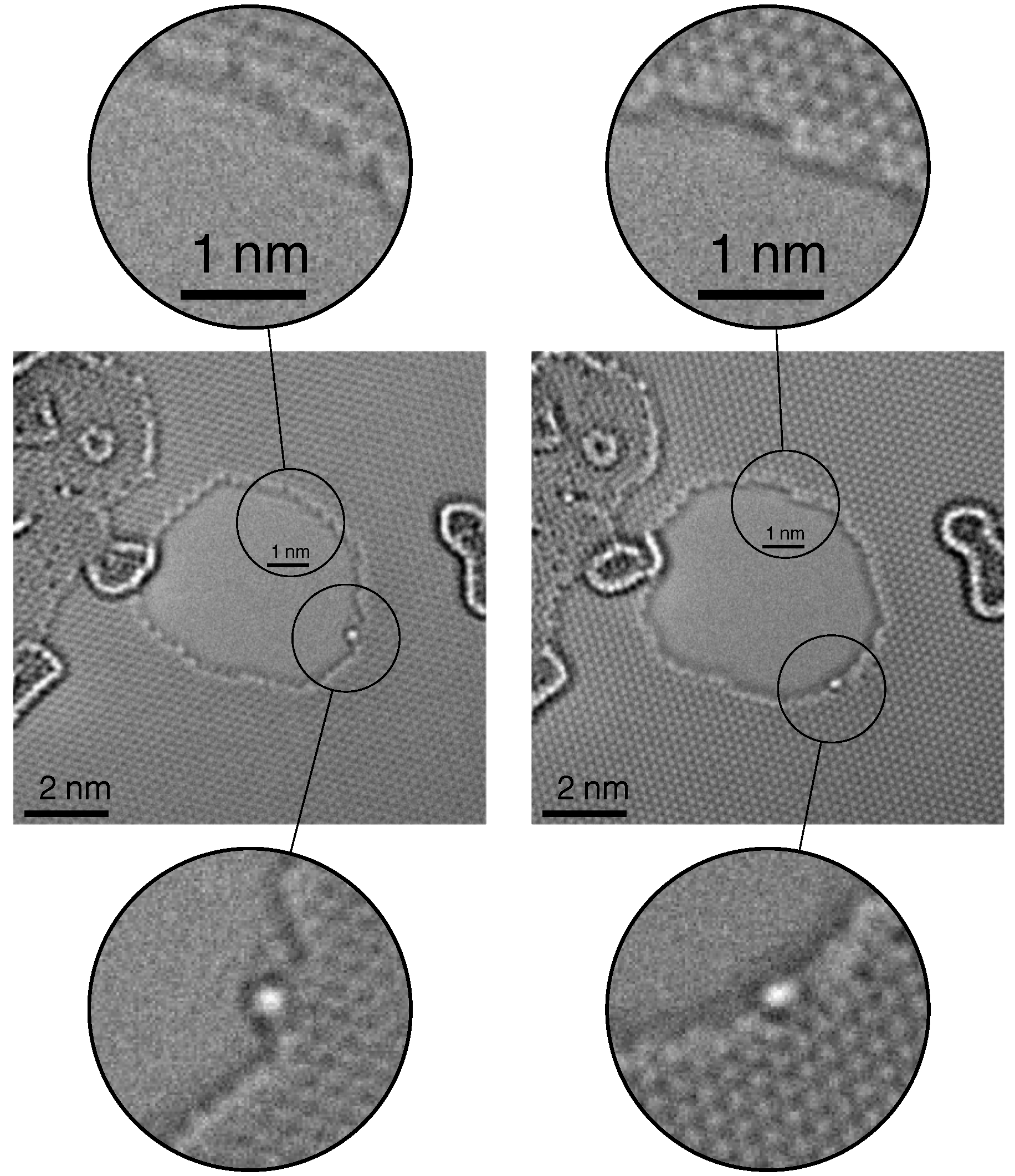
In order to "use" the transferred information in a proper way, the phase plate, i.e. the aberration function, has been well-controlled beyond the 50 mrad-angle. This requires accurate control over axial aberrations up to including 5th order, and - for a considerable field of view - access to off-axial aberrations. All unround axial aberrations as well as the off-axial aberrations can be tuned sufficiently small. At the same time, the round aberrations can be adjusted for a suitable phase contrast transfer function. Fig. 2 shows atomic resolution in raw micrographs of graphene with adatoms and edges at 20 kV.

The performance of the SALVE III microscope thus enables atomic-resolution imaging and high-resolution energy-filtered (EF)-TEM with large energy windows even at 20 kV accelerating voltage [1 - 2]. It is capable to image a 20 eV window with defocus changes of only 2 nm. The reduced axial brightness of the FEI X-FEG Schottky type with a (switched off) monochromator was determined to be larger than 1.8 x 10⁸ A/(m2 sr V). The illumination semi-angle distribution. For the different dose rate conditions, we get a dose rate of 3,500 e−/(Å2 s) with an illumination semi-angle distribution of 70 μrad at 20 kV and 110 μrad at 80 kV. Under low dose rate conditions of 34 e−/(Å2 s) which is a value typically used in imaging biological samples, the illumination semi-angle distribution is 7 μrad at 20 kV. [3]
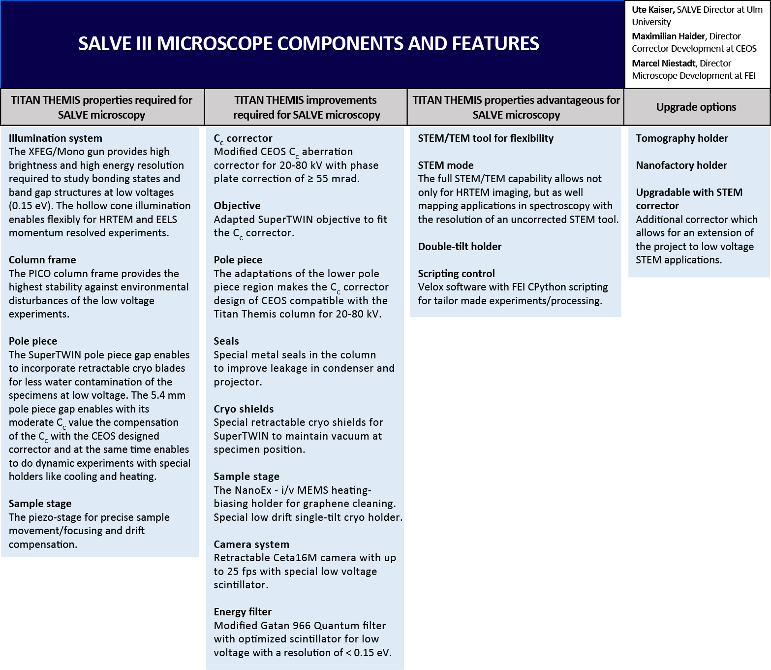
A major part of SALVE III concerned the incorporation of the corrector in the FEI Titan Themis TEM. The microscope column and power meets the stringent requirements of the operation at low voltages. It has been further optimized in many components to tailor the system for the low voltage microscopy application. This does not only include the Cc corrector but involves also the other components such as an improved vacuum system, cryo shields and new stable specimen holders. It exceed the performance of the Titan Themis with special features for the low voltage applications. An overview this is given in Fig. 3.
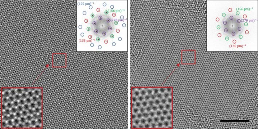
As shown in Figs. 2 and 4, even at very low accelerating voltage atomic resolution imaging becomes reality. Fig. 4 demonstrates good agreement of experimental and calculated image. [4]

As shown in Fig. 5 the resolution obtained with the Cc/Cs corrected SALVE III microscope at 30 kV for 2D MoS2 is higher by about a factor of 2 than the resolution obtained with Cs-corrected microscopes at 80 kV earlier [5].

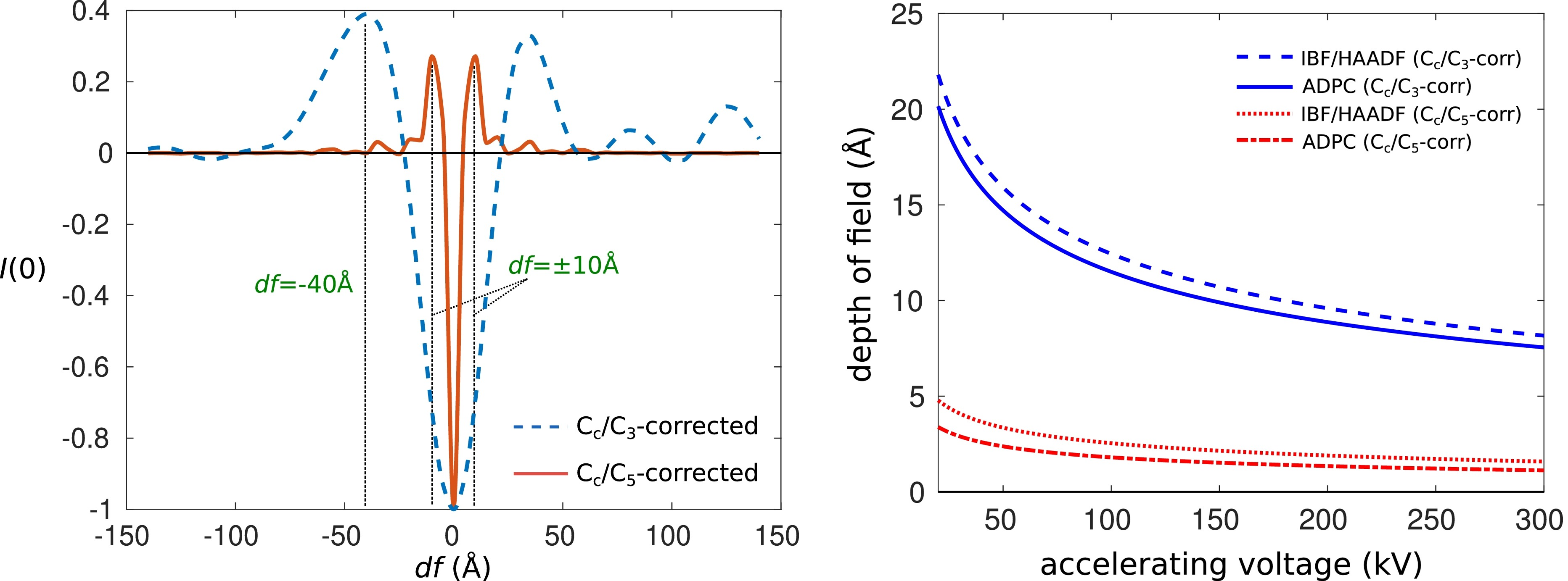
As shown in Fig. 6 by image calculation we explored the feasibility of the annular differential phase contrast (ADPC) and compare to the incoherent bright-field (IBF) and high-angle annular dark-field (HAADF) Cc/C3 and Cc/C5 STEM mode. [6]

Summary
A TEM equipped with a CC/CS-corrector can be used for atomic imaging down to 20 kV. Aberrations are sufficiently small to allow for phase contrast imaging between 55 and 67 mrad. With this microscope SALVE III has now further advanced the technique in aberration-corrected low-voltage transmission electron microscopy.
Linck, M., Hartel, P., Uhlemann, S., Kahl, F., Müller, H., Zach, J., Haider, M., Niestadt, M., Bischoff, M., Biskupek, J., Lee, Z., Lehnert, T., Börrnert, F., Rose, H. H. & Kaiser, U. A. (2016). Chromatic Aberration Correction for Atomic Resolution TEM Imaging from 20 to 80 kV. Physical Review Letters, 117: 076101, doi: 10.1103/PhysRevLett.117.076101
Börrnert, F., & Kaiser, U. (2018). Chromatic-and geometric-aberration-corrected TEM imaging at 80 kV and 20 kV. Physical Review A, 98: 023861, doi: 10.1103/PhysRevA.98.023861
Börrnert, F., Renner, J., & Kaiser, U. (2018). Electron Source Brightness and Illumination Semi-Angle Distribution Measurement in a Transmission Electron Microscope. Microscopy and Microanalysis, 24: 249-255, doi: 10.1017/S1431927618000223
Kaiser, U. (2016). Properties of low-dimensional electron-beam-sensitive objects by spherical and chromatic aberration-corrected low-voltage high-resolution transmission electron microscopy and spectroscopy. In: The 15th European Microscopy Congress (John Wiley & Sons, Germany, 2016): 8679, doi: 10.1002/9783527808465.EMC2016.8679
Lehnert, T., Biskupek, J., Köster, J., Linck, M., & Kaiser, U. (2016). Quantitative low-voltage spherical and chromatic aberration-corrected high-resolution TEM analysis of beam-specimen interactions in single-layer MoS2 and MoS2/graphene heterostructures. In: The 15th European Microscopy Congress (John Wiley & Sons, Germany, 2016): 5742, doi: 10.1002/9783527808465.EMC2016.5738
Lee, Z., Kaiser, U., & Rose, H. (2019). Prospects of annular differential phase contrast applied for optical sectioning in STEM. Ultramicroscopy, 196: 58-66., doi: 10.1016/j.ultramic.2018.09.012

