Towards Quantum Devices: Single-Layer MoTe2 under the electron beam.
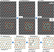
April 26, 2019 – Scientists have revealed new point and line defects in monolayer MoTe2 in the electron microscope. With the Cc/Cs-corrected SALVE TEM at 40 kV electron acceleration voltage [1-3] they locate and produce the defects in the 2D material. They then used first-principles simulations to provide insights into their electronic and magnetic properties. As such defects possess interesting band structure and magnetic moments, the accomplishment sets the stage for future quantum devices (Figure 1).
Transition metal dichalcogenides (TMDs) such as MoTe2 can be insulators, semiconductors, metals, superconductors, or charge density waves. [4-6] They can be produced by exfoliation [4] or grown by chemical vapor deposition,[7] and have been shown to have numerous practical applications. [8] They can be modified and imaged at the same time in a TEM under the electron beam. [9-13]
Their agglomeration can drastically change their properties. [5,8,14] such as becoming catalytically active centers. [15] In particular the highly symmetric mirror twin boundaries (MTBs) [16-18] can constitute a one-dimensional metallic quantum object in a semiconducting matrix. [19] However, it was not clear what role point defects play in MTB formation or how mechanical strain affects their formation. The exact structure and directions can be quite different, [20,21] and the reason for this remained elusive, because the resolution of conventional electron microscopes is insufficient to resolve these defects at the atomic scale.
Scientists at the University of Ulm and the Helmholtz-Zentrum Dresden-Rossendorf in Germany as well as the University of Aalto in Finland have now made a comprehensive new atomic scale study with the Cc/Cs corrected SALVE microscope that provides atomic resolution at 40 kV. They captured the defect formation and evolution in a more realistic way than previous efforts and carried out supportive DFT calculations. The new observation include several defects which have never been observed before. The research is also relevant for other TMDs, [20-23] as the relation between the atomic structure [16] of the emerging MTBs and the experimental conditions [21,23] was revealed for the first time.
“With the combination of first-principles calculations we are explaining the defect formation, migration, and their coalescence resulting ultimately in the formation of inversion domains,” said Ute Kaiser, professor at the Electron Group of Materials Science (EMMS) in Ulm and at the SALVE microscopy center. “The controllable introduction of particular defects that introduce certain functionalities may be used application-related for devices with new optical, electronic, and magnetic properties.”
Migrating the defects
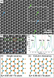
For the new study, the scientists had to build on a TEM where differences between the contrast of a single missing Te atom produces still a slightly higher signal than a neighboring Mo atom (Figure 2). With a resolution of 0.9 Å the capturing of the complex physical behavior of the defective MoTe2 was carried out at an acquisition time of ∼1 s at an extremely large field of view. [2] Furthermore, atom "knock-on" should be impossible at 40 kV.[24] The maximum transferable kinetic energy is 0.72 eV for Te atoms and 0.95 eV for Mo atoms. In contrast, the energy of formation of a defect site for Te is around 4.87 eV and for Mo 10.45 eV. Actual values could be even higher. [24]
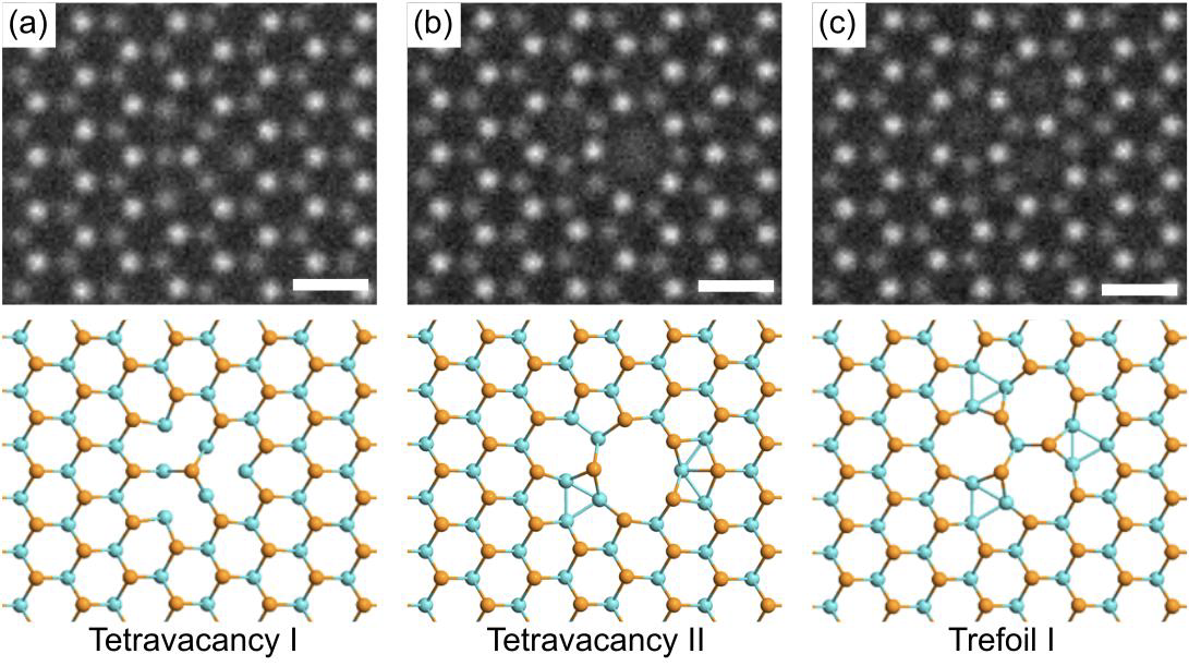
At the low acceleration voltage, the formation of more complicated defects where several atoms are missing has been observed. The exact mechanism of defect formation is not known, however water fragments in the TEM could likely be a main reason as they could introduce material damage via chemical etching. [25] (Figure 3, Highlighted Topic 1). These defects are called “extended point defects”, as they are slightly larger than single vacancies. The formation of such defects starts with two column Te divacancies which migrate into a symmetric defect. A distortion can than take place and turn a tetravacancy I into a tetravacancy II (Figure 3b). After further electron irradiation and additional Te2 vacancy formation, the distorted tetravacancy II can be transformed into the trefoil I structure (Figure 3c). Because of a bond rotation, other types of tetravacancy and trefoil defects can eventually be formed such as tetravacancies III and IV and trefoil II (see Highlighted Topic 1).
To successfully study the electronic and magnetic properties of the defects, the scientists needed to calculate the spin-polarized total density of states (DOS). The presence of defects significantly changes the electronic structure and introduces a large number of midgap states which act as scattering centers affecting the electronic transport properties. The calculations revealed that the shift between the spin-up and spin−down states in the tetravacancy I and II has a magnetic character. While pristine MoTe2 is nonmagnetic, [26] these defects possess a total magnetic moment of > 2 μB. Such a defect embedded into a semiconducting matrix is called a quantum dot.
"We have a situation, where subsequent TEM imaging also results in line defect formation" said Ute Kaiser. "However, also for the extended defects, the comparison of the atom positions between experimental and simulated images today can provide understanding of the properties of the materials."
The interaction of the electron beam with the MoTe2 specimen resulted also in line defect formation (Figure 4). To analyze the system that appeared in the TEM, the spin-polarized total density of states (DOS) was calculated (Figure 5), which needed to be both realistic and computationally efficient. According to the calculations, different line defects can be interpreted as band gap reduction as compared to the pristine structure, provided that the concentration of vacancy lines is high. However, line defects can be regarded as quantum wires because of confined metallic properties within the semiconducting MoTe2. Spatial localization of spin up and down electron density indicates that some of these metallic structures could be used in spintronics.
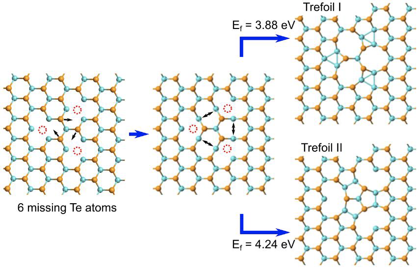
The next step was to understand if the structural evolution of the defects under the electron beam can be described in terms of the energetics of defects of various types (Figure 6). In previous research using re-doped MoS2 [5]similar transformations had already been observed. The transformations likely originate from strain induced by vacancies and possibly other effects related to charge transfer and vibrational properties. [27,28] In the new study, the team found out that in the case of the single Te vacancies, the formation of lines is energetically favored. In the case of column Te divacancies their agglomeration to lines is only slightly preferred but their agglomeration to extended point defects releases a substantial amount of energy (Figure 6). Some defects were not observed earlier in MoTe2. Figure 7 shows a single Te vacancy line with six missing Te atoms. The displacements of Te atoms, led to a formation of an island of 1T′ phase in (e). The scientists tried to analyze the single vacancy line that moved along a distance of two unit cells.
“Finally. using the 40 kV electron beam we were able to provide insights into the formation and evolution process of inversion domains with mirror twin boundaries of different types, along with the islands of the metallic phases that occur,” Kaiser said.
Now that the study has shown the various nanoscale morphologies, including metallic islands of the T′ phase, and one-dimensional metallic systems based on vacancy lines and mirror twin boundaries, the next step is to realize quantum devices using single-layer MoTe2.
“We showed that some of the observed defects have localized magnetic moments,” Kaiser said. “This may lead toward control of optical and electronic properties for quantum devices in 2D materials. Other systems that we observed are very interesting in the context of fundamental aspects of physics and for practical aspects in plasmonics.”
Resource: Lehnert, T., Ghorbani-Asl, M., Köster, J., Lee, Z., Krasheninnikov, A. V., & Kaiser, U. A. (2019). Electron-Beam-Driven Structure Evolution of Single-Layer MoTe2 for Quantum Devices. ACS Appl. Nano Mater., 5, 3262-3270, doi: 10.1021/acsanm.9b00616, [PDF], see also the supporting information.
Kaiser, U.; Biskupek, J.; Meyer, J. C.; Leschner, J.; Lechner, L.; Rose, H.; Stöger-Pollach, M.; Khlobystov, A. N.; Hartel, P.; Müller, H.; Haider, M.; Eyhusen, S.; Benner, G. Transmission electron microscopy at 20 KV for imaging and spectroscopy. Ultramicroscopy 2011, 111 (8), 1239−1246.
Linck, M.; Hartel, P.; Uhlemann, S.; Kahl, F.; Müller, H.; Zach, J.; Haider, M.; Niestadt, M.; Bischoff, M.; Biskupek, J.; Lee, Z.; Lehnert, T.; Börrnert, F.; Rose, H.; Kaiser, U. Chromatic aberration correction for atomic resolution TEM imaging from 20 to 80 KV. Phys. Rev. Lett. 2016, 117, 076101.
Lee, Z.; Meyer, J. C.; Rose, H.; Kaiser, U. Optimum HRTEM image contrast at 20 KV and 80 KV – exemplified by graphene. Ultramicroscopy 2012, 112 (1), 39−46.
Chhowalla, M.; Shin, H. S.; Eda, G.; Li, L.-J.; Loh, K. P.; Zhang, H. The chemistry of two-dimensional layered transition metal dichalcogenide nanosheets. Nat. Chem. 2013, 5 (4), 263.
Lin, Y.-C.; Dumcenco, D. O.; Huang, Y.-S.; Suenaga, K. Atomic mechanism of the semiconducting-to-metallic phase transition in single-layered MoS2. Nat. Nanotechnol. 2014, 9 (5), 391.
Wilson, J. A.; Di Salvo, F. J.; Mahajan, S. Charge-density waves and superlattices in the metallic layered transition metal dichalcogenides. Adv. Phys. 1975, 24 (2), 117−201.
Wang, Q. H.; Kalantar-Zadeh, K.; Kis, A.; Coleman, J. N.; Strano, M. S. Electronics and optoelectronics of two-dimensional transition metal dichalcogenides. Nat. Nanotechnol. 2012, 7 (11), 699.
Deng, K.; Wan, G.; Deng, P.; Zhang, K.; Ding, S.; Wang, E.; Yan, M.; Huang, H.; Zhang, H.; Xu, Z.; Denlinger, J.; Fedorov, A.; Yang, H.; Duan, W.; Yao, H.; Wu, Y.; Fan, S.; Zhang, H.; Chen, X.; Zhou, S. Experimental observation of topological fermi arcs in type-II Weyl semimetal MoTe2. Nat. Phys. 2016, 12 (12), 1105.
Zhao, X.; Kotakoski, J.; Meyer, J. C.; Sutter, E.; Sutter, P.; Krasheninnikov, A. V.; Kaiser, U.; Zhou, W. Engineering and modifying two-dimensional materials by electron beams. Mrs Bulletin 2017, 42(9), 667-676.
Kalinin, S. V.; Pennycook, S. J. Single-atom fabrication with electron and ion beams: From surfaces and two-dimensional materials toward three-dimensional atom-by-atom assembly. MRS Bulletin 2017, 42(9), 637-643.
Susi, T.; Meyer, J. C.; Kotakoski, J. Manipulating low-dimensional materials down to the level of single atoms with electron irradiation. Ultramicroscopy 2017, 180, 163-172.
Susi, T.; Meyer, J. C.; Kotakoski, J. Quantifying transmission electron microscopy irradiation effects using two-dimensional materials. Nature Reviews Physics 2019, 1, 397-405.
Dyck, O.; Ziatdinov, M.; Lingerfelt, D. B.; Unocic, R. R.; Hudak, B. M.; Lupini, A. R.; Jesse, S.; Kalinin, S. V. Atom-by-atom fabrication with electron beams. Nature Reviews Materials 2019, 4, 497-507.
Cho, S.; Kim, S.; Kim, J. H.; Zhao, J.; Seok, J.; Keum, D. H.; Baik, J.; Choe, D.-H.; Chang, K. J.; Suenaga, K.; Kim, S. W.; Lee, Y. H.; Yang, H. Phase patterning for Ohmic homojunction contact in MoTe2. Science 2015, 349 (6248), 625−628.
Kosmala, T.; Coy Diaz, H.; Komsa, H.-P.; Ma, Y.; Krasheninnikov, A. V.; Batzill, M.; Agnoli, S. Metallic twin boundaries boost the hydrogen evolution reaction on the basal plane of molybdenum selenotellurides. Adv. Energy Mater. 2018, 8, 1800031.
Komsa, H.-P.; Krasheninnikov, A. V. Engineering the electronic properties of two-dimensional transition metal dichalcogenides by introducing mirror twin boundaries. Adv. Electron. Mater. 2017, 3 (6), 1600468.
Ma, Y.; Kolekar, S.; Coy Diaz, H.; Aprojanz, J.; Miccoli, I.; Tegenkamp, C.; Batzill, M. Metallic twin grain boundaries embedded in MoSe2 monolayers grown by molecular beam epitaxy. ACS Nano 2017, 11 (5), 5130−5139.
Lehtinen, O.; Komsa, H.-P.; Pulkin, A.; Whitwick, M. B.; Chen, M.-W.; Lehnert, T.; Mohn, M. J.; Yazyev, O. V.; Kis, A.; Kaiser, U.; Krasheninnikov, A. V. Atomic scale microstructure and properties of Se-deficient two-dimensional MoSe2. ACS Nano 2015, 9 (3), 3274−3283.
Barja, S.; Wickenburg, S.; Liu, Z.-F.; Zhang, Y.; Ryu, H.; Ugeda, M. M.; Hussain, Z.; Shen, Z.-X.; Mo, S.-K.; Wong, E.; Salmeron, M. B.; Wang, F.; Crommie, M. F.; Ogletree, D. F.; Neaton, J. B.; Weber-Bargioni, A. Charge density wave order in 1D mirror twin boundaries of single-layer MoSe2. Nat. Phys. 2016, 12, 751−756.
Algara-Siller, G.; Kurasch, S.; Sedighi, M.; Lehtinen, O.; Kaiser, U. The pristine atomic structure of MoS2 monolayer protected from electron radiation damage by graphene. Appl. Phys. Lett. 2013, 103, 20307.
Wang, S.; Lee, G.-D.; Lee, S.; Yoon, E.; Warner, J. H. Detailed atomic reconstruction of extended line defects in monolayer MoS2. ACS Nano 2016, 10 (5), 5419−5430.
Pizzochero, M.; Yazyev, O. V. Point defects in the 1 T′ and 2 H phases of single-layer MoS2: A comparative first-principles study. Phys. Rev. B: Condens. Matter Mater. Phys. 2017, 96 (24), 245402.
Komsa, H.-P.; Kurasch, S.; Lehtinen, O.; Kaiser, U.; Krasheninnikov, A. V. From point to extended defects in two-dimensional MoS2: Evolution of atomic structure under electron irradiation. Phys. Rev. B: Condens. Matter Mater. Phys. 2013, 88, 035301.
Komsa, H.-P.; Kotakoski, J.; Kurasch, S.; Lehtinen, O.; Kaiser, U.; Krasheninnikov, A. V. Two-dimensional transition metal dichalcogenides under electron irradiation: Defect production and doping. Phys. Rev. Lett. 2012, 109, 035503.
Meyer, J. C.; Eder, F.; Kurasch, S.; Skakalova, V.; Kotakoski, J.; Park, H. J.; Roth, S.; Chuvilin, A.; Eyhusen, S.; Benner, G.; Krasheninnikov, A. V.; Kaiser, U. Accurate measurement of electron beam induced displacement cross sections for single-layer graphene. Phys. Rev. Lett. 2012, 108 (19), 196102.
Ataca, C.; Sahin, H.; Akturk, E.; Ciraci, S. Mechanical and Electronic Properties of MoS2 Nanoribbons and Their Defects. J. Phys. Chem. C 2011, 115 (10), 3934−3941.
Duerloo, K.-A. N.; Li, Y.; Reed, E. J. Structural phase transitions in two-dimensional Mo-and W-dichalcogenide monolayers. Nat. Commun. 2014, 5, 4214.
Kretschmer, S.; Komsa, H.-P.; Bøggild, P.; Krasheninnikov, A. V. Structural transformations in two-dimensional transition-metal dichalcogenide MoS2 under an electron beam: Insights from first-principles calculations. J. Phys. Chem. Lett. 2017, 8 (13), 3061−3067.
Perdew, J. P.; Burke, K.; Ernzerhof, M. Generalized gradient approximation made simple. Phys. Rev. Lett. 1996, 77 (18), 3865.
Kresse, G.; Furthmüller, J. Efficiency of ab-initio total energy calculations for metals and semiconductors using a plane-wave basis set. Comput. Mater. Sci. 1996, 6 (1), 15−50.


