Pressure alters the band structure of 2D Platinum dichalcogenides
August 16, 2021 - Platinum dichalcogenides exhibit tunability of their electronic properties displaying semimetal to semiconductor transition as they are reduced to bi- or single layers. Scientists from the University of South Florida in the United States as well as the Helmholtz-Zentrum Dresden-Rossendorf and the University of Ulm in Germany have grown monolayer and multilayer Pt dichalcogenides on graphene, characterized the samples on the atomic scale and analyzed their band gap. The results show that pressure can significantly reduce the band gap, making Pt dichalcogenides suitable materials for pressure sensing.
The thickness and dimension of layered transition metal dichalcogenides (TMDs) [1] with their strong in-plane covalent bonding and weak van der Waals interaction between molecular planes can exhibit a strong impact on their electronic structure.[2-5] Density functional theory (DFT) calculations have suggested that interlayer interactions may be particularly strong in the Pt dichalcogenides.[6-8] Band gaps of 1.18 and 0.24 eV have been predicted for monolayer and bilayer PtSe2, respectively. For monolayer PtTe2, a 0.4 eV band gap has been predicted, while bilayer PtTe2 was predicted to remain (semi)metallic. In the bulk, PtS2 is semiconducting. For PtSe2 previously reported theoretical values of the gap gave different results.[7]
The new research draws on observations by advanced microscopic techniques, aberration-corrected high-resolution transmission electron microscopy (AC-HRTEM) and scanning tunneling spectroscopy (STS) to quantify the defects and number of layers on the atomic scale and obtain the first experimental observation of the band gap of Pt dichalcogenides. DFT simulations are then used to analyze what is causing the electronic structure of the layered and monolayer materials.
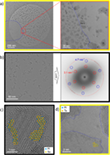
To characterize the Pt chalcogenides, the authors grew the films directly on suspended graphene on a TEM grid by molecular beam epitaxy (MBE). To investigate the samples at the atomic scale, they were first annealed in the TEM to desorb some adsorbates from the air exposure at 200 °C for 30 min, but nevertheless, more carbon decorating the PtSe2 and the PtTe2 edges was detected. TEM characterization confirmed the formation of the Pt chalcogenides on the graphene sheet (Figure 1a). The distribution of lateral island areas is about 30–100 nm2 in one region and 100–650 nm2 in another. The regions with the smaller islands are like those grown in situ on HOPG, and thus, these regions are considered to have been contamination-free during growth, while the larger islands are likely formed by adsorption and agglomeration at pre-existing contamination on the graphene. All the regions show carbon contamination, which is expected to have occurred during post-growth air exposure. The island heights vary from monolayer to multilayers. Some bilayer islands were also formed (Figure 1c).
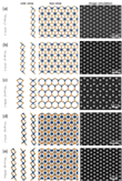
While the image contrast allows one to exclude the possibility of the 2H phase for both monolayer and bilayers, the contrast differences between different stackings of the 1T layers in the bilayers, i.e., 1T or 3R stacking, are small (Figure 2) and do not allow one to unambiguously differentiate between these stackings from image contrast alone. However, the Se and Pt sublattices and the number of layers were found from often observed Se vacancies by analyzing line scans along the Pt and Se atoms as shown in Figure 3. In combination with the line scans (Figure 3), the HRTEM images as well as the simulated images of different possible structures (Figure 2) show the formation of bilayer PtSe2 with a 1T structure.
The research team then applied DFT calculations. The 1T structure has been expected to be thermodynamically most stable for both PtSe2 and PtTe2, [9] and this could be confirmed (Figure 4). Thus, DFT and selected TEM image analyses are consistent with a majority of 1T stacked bilayer islands. The Fourier transformation shows a lattice constant of PtSe2 = 0.38 nm (Figure 1b) were consistent with the previously reported data.[10, 11]Interestingly, despite the weak van der Waals interactions between graphene and PtSe2, the PtSe2 islands grow epitaxially on the graphene substrate, i.e., the hexagonal lattice of the islands is aligned with respect to the hexagonal structure of graphene. The HRTEM images of MBE grown PtTe2 islands are similar in many respects to those of PtSe2 (Figure 1d). The monolayer 1H phase would show a metallic character according to the DFT simulations, and thus, no band gap opening would be expected.
Pure DFT level calculations showed that the band gap value of monolayer PtSe2 is not affected by a graphene substrate. This was surprising as band gap renormalization has been discussed extensively for TMDs on metal supports mainly for the Mo dichalcogenides.[12] On pure transition metals, such as Au, a strong decrease of the fundamental band gap compared to free-standing material is seen.[13] However, on weakly interacting substrates such as graphene or graphite, the situation is less clear though. For MoS2, for example, the measured gaps vary between 2.15 and 2.4 eV for graphite [14] or 2.53 eV for graphene/Ir [15] substrates, while some DFT calculations predicted gaps as large as 2.8 eV for the monolayer.[16] For the DFT calculations, the PtSe2/graphene heterostructure was constructed with 3 × 3 unit cells of graphene and 2 × 2 unit cells of the PtSe2 monolayer corresponding to a lattice mismatch of only 0.7% (Figure 5).
Structural optimization with many-body dispersion correction led to an average interlayer distance of d = 3.47 Å between PtSe2 and graphene. The band structure of the heterostructure showed a linear energy dispersion close to the Fermi level resembling the Dirac cone of graphene. The projected densities of states suggest that the band gap of the PtSe2 monolayer on graphene is like that of the free-standing monolayer, showing that Pt dichalcogenides supported on graphitic substrates are good models for qualitative analysis of the electronic properties of the free-standing layers. To further test the influence of the substrate on the band gap, the separation between graphene and PtSe2 was artificially reduced by up to 10% of its equilibrium separation and the gap value was re-evaluated (Figure 6). It is also noteworthy that interface band alignment in the graphene/PtSe2 system causes a slight shift of the Fermi level toward the conduction band in the DFT calculations associated with a small charge transfer to PtSe2 (Figure 7).
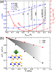
The scientists further investigated the response of the bilayer system under compression applied perpendicularly to the surface. The PtSe2 bilayer was subjected to a normal compressive load in a “displacement regulation simulation”, in which the equilibrium interlayer distance is systematically reduced in steps and the total energy is recalculated. The energies and the area of the interface were used to calculate the applied pressure (P) at each step. The band gap evolution under applied compression showed almost linear behavior with increasing pressure (Figure 8b). The pressure-induced band gap change in PtSe2 is more pronounced in the comparison to group VI TMDs such as MoSe2, [17] suggesting that noble TMDs are promising materials for pressure-tunable optoelectronic devices or sensors.
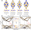
The 1T Pt dichalcogenides can be grown by MBE as epitaxially aligned islands on various graphitic substrates. On HOPG, individual islands expose multiple terrace heights, thus enabling one to measure the electronic property variation as a function of the number of layers by STS. The STS observations showed that the lattice constants were in good agreement with the experimental values (Table S1). Also the charge transfer was experimentally seen. A slight n-type doping was measured for PtSe2 monolayers by STS. A good agreement with the experimental band structure measurements from STS is obtained only if spin–orbit coupling (SOC) is included in the calculations as shown for the monolayer (Figure 9e) and the bilayer (Figure 9f). An overlay of the experimental band structure with the calculated bands is also shown. This good agreement confirmed the DFT approach. The calculations show that monolayer PtTe2 and PtSe2 exhibit an indirect band gap with the VBM at the Γ point and the CBM at low symmetry points along the Γ–M direction. The calculated band structures were also in good agreement with the experimental ARPES data for PtTe2 mono- and bilayer samples.
The analysis showed that PtSe2 and PtTe2 monolayers have an indirect band gap of 1.20 and 0.33 eV, respectively. The application of quasi-particle band gap calculations at the G0W0 (single-shot GW) level increased the band gap of PtSe2 (PtTe2) to 2.44 eV (1.29 eV). These values are normally overestimations of the band gaps for the free-standing monolayers. [18] As PBE usually underestimates band gaps, one can assume that the experimental values are between the PBE and the G0W0 values, in agreement with the experimental data. The calculated band gaps are also in good agreement with the previously reported values at a similar level of theory. [6],[19] The increase of the number of layers from mono- to bilayer leads to a significant reduction of the calculated band gaps and gives rise to a semimetallic behavior for the trilayer and beyond, confirming the strong interlayer interaction in these materials. The study further verified that in multilayer systems, the chosen vdW correction method has a major influence on the calculated band gap. While the DFT+D3 method turns out to underestimate the distance between layers, more advanced TS and MBD corrections increase the interlayer distance, approaching the experimental range of 5.08–5.3 Å (Figure 8a).
For PtSe2, a transition from a metal for more than a 3-layer thick island to a semiconductor is seen, while for PtTe2, the transition from metal to semiconductor occurs only for the monolayer. The fundamental band gaps have been decided experimentally by STS, which shows that monolayers of PtSe2 and PtTe2 exhibit significant indirect band gaps of 1.8 and 0.5 eV, respectively. DFT calculations reproduce the general trend of opening of a gap as the number of layers is reduced. The strong layer dependence of the fundamental band gap in PtSe2 and PtTe2 is attributed to the interlayer interactions, which are stronger than in other TMDs.
”The sensitivity of the band gap to interlayer separation allowed us to propose that the band gap can be tuned by uniaxial compression of the bilayer systems.” said the authors. “Our theoretical studies suggest that significant modifications of the band gap in bilayer PtSe2 can be obtained with modest pressure of less than 1 GPa, making it a feasible system for stress sensors or stress-tunable optoelectronic devices.”
Resource: Jingfeng Li, Sadhu Kolekar, Mahdi Ghorbani-Asl, Tibor Lehnert, Johannes Biskupek, Ute A. Kaiser, Arkady V. Krasheninnikov & Matthias Batzill. Layer-Dependent Band Gaps of Platinum Dichalcogenides (2021) ACS Nano 15, 13249-13259, doi: 10.1021/acsnano.1c02971, [PDF], see also the supporting information.
-
Lasek, K.; Li, J.; Kolekar, S.; Coelho, P. M.; Zhang, M.; Wang, Z.; Batzill, M. Synthesis and characterization of 2D transition metal dichalcogenides: recent progress from a vacuum surface science perspective. Surf. Sci. Rep. 2021, 76, 100523.
-
Mak, K. F.; Lee, C.; Hone, J.; Shan, J.; Heinz, T. F. Atomically thin MoS2: a new direct-gap semiconductor. Phys. Rev. Lett. 2010, 105, 136805.
-
Kolekar, S.; Bonilla, M.; Ma, Y.; Diaz, H. C.; Batzill, M. Layer-and substrate-dependent charge density wave criticality in 1T-TiSe2. 2D Mater. 2018, 5, 015006.
-
Coelho, P. M.; Cong, K. N.; Bonilla, M.; Kolekar, S.; Phan, M.-H.; Avila, J.; Asensio, M. C.; Oleynik, I. I.; Batzill, M. Charge density wave state suppresses ferromagnetic ordering in VSe2 monolayers. J. Phys. Chem. C 2019, 123, 14089– 14096.
-
Duvjir, G.; Choi, B. K.; Jang, I.; Ulstrup, S.; Kang, S.; Ly, T. T.; Kim, S.; Choi, Y. H.; Jozwiak, C.; Bostwick, A.; Rotenberg, E.; Park, J.-G.; Sankar, R.; Kim, K.-S.; Kim, J.; Chang, Y. J. Emergence of a metal-insulator transition and high-temperature charge-density waves in VSe2 at the monolayer limit. Nano Lett. 2018, 18, 5432– 5438.
-
Villaos, R. A. B.; Crisostomo, C. P.; Huang, Z.-Q.; Huang, S.-M.; Padama, A. A. B.; Albao, M. A.; Lin, H.; Chuang, F.-C. Thickness dependent electronic properties of Pt dichalcogenides. npj 2D. Mater. Appl. 2019, 3, 2.
-
Zhao, Y.; Qiao, J.; Yu, P.; Hu, Z.; Lin, Z.; Lau, S. P.; Liu, Z.; Ji, W.; Chai, Y. Extraordinarily strong interlayer interaction in 2D layered PtS2. Adv. Mater. 2016, 28, 2399– 2407.
-
Zhao, Y.; Qiao, J.; Yu, Z.; Yu, P.; Xu, K.; Lau, S. P.; Zhou, W.; Liu, Z.; Wang, X.; Ji, W.; Chai, Y. High-electron-mobility and air-stable 2D layered PtSe2 FETs. Adv. Mater. 2017, 29, 1604230.
-
Miró, P.; Ghorbani-Asl, M.; Heine, T. Two dimensional materials beyond MoS2: Noble-transition-metal dichalcogenides. Angew. Chem., Int. Ed. 2014, 53, 3015– 3018.
-
Shi, J.; Huan, Y.; Hong, M.; Xu, R.; Yang, P.; Zhang, Z.; Zou, X.; Zhang, Y. Chemical vapor deposition grown large-scale atomically thin platinum diselenide with semimetal-semiconductor transition. ACS Nano 2019, 13, 8442– 8451.
-
Zhou, J.; Kong, X.; Sekhar, M. C.; Lin, J.; Le Goualher, F.; Xu, R.; Wang, X.; Chen, Y.; Zhou, Y.; Zhu, C.; Lu, W.; Liu, F.; Tang, B.; Guo, Z.; Zhu, C.; Cheng, Z.; Yu, T.; Suenaga, K.; Sun, D.; Ji, W.; Liu, Z. Epitaxial synthesis of monolayer PtSe2 single crystal on MoSe2 with strong interlayer coupling. ACS Nano 2019, 13, 10929– 10938.
-
Ugeda, M. M.; Bradley, A. J.; Shi, S.-F.; da Jornada, F. H.; Zhang, Y.; Qiu, D. Y.; Ruan, W.; Mo, S.-K.; Hussain, Z.; Shen, Z.-X.; Wang, F.; Louie, S. G.; Crommie, M. F. Giant bandgap renormalization and excitonic effects in a monolayer transition metal dichalcogenide semiconductor. Nat. Mater. 2014, 13, 1091– 1095.
-
Bruix, A.; Miwa, J. A.; Hauptmann, N.; Wegner, D.; Ulstrup, S.; Grønborg, S. S.; Sanders, C. E.; Dendzik, M.; Čabo, A. G.; Bianchi, M.; Lauritsen, J. V.; Khajetoorians, A. A.; Hammer, B.; Hofmann, P. Single-layer MoS2 on Au(111): band gap renormalization and substrate interaction. Phys. Rev. B: Condens. Matter Mater. Phys. 2016, 93, 165422.
-
Zhang, C.; Johnson, A.; Hsu, C. L.; Li, L.-J.; Shih, C.-K. Direct imaging of band profile in single Layer MoS2 on graphite: quasiparticle energy gap, metallic edge states, and edge band bending. Nano Lett. 2014, 14, 2443– 2447.
-
Murray, C.; Jolie, W.; Fischer, J. A.; Hall, J.; van Efferen, C.; Ehlen, N.; Grüneis, A.; Busse, C.; Michely, T. Comprehensive tunneling spectroscopy of quasi-freestanding MoS2 on graphene on Ir(111). Phys. Rev. B: Condens. Matter Mater. Phys. 2019, 99, 115434.
-
Qiu, D. Y.; da Jornada, F. H.; Louie, S. G. Optical spectrum of MoS2: many-body effects and diversity of exciton states. Phys. Rev. Lett. 2013, 111, 216805.
-
Zhao, Z.; Zhang, H.; Yuan, H.; Wang, S.; Lin, Y.; Zeng, Q.; Xu, G.; Liu, Z.; Solanki, G. K.; Patel, K. D.; Cui, Y.; Hwang, H. Y.; Mao, W. L. Pressure induced metallization with absence of structural transition in layered molybdenum Diselenide. Nat. Commun. 2015, 6, 7312.
-
Rasmussen, F. A.; Schmidt, P. S.; Winther, K. T.; Thygesen, K. S. Efficient many-body calculations for two-dimensional materials using exact limits for the screened potential: band gaps of MoS2, h-BN, and phosphorene. Phys. Rev. B: Condens. Matter Mater. Phys. 2016, 94, 155406.
-
Wang, Y.; Li, L.; Yao, W.; Song, S.; Sun, J. T.; Pan, J.; Ren, X.; Li, C.; Okunishi, E.; Wang, Y.-Q.; Wang, E.; Shao, Y.; Zhang, Y. Y.; Yang, H. T.; Schwier, E. F.; Iwasawa, H.; Shimada, K.; Taniguchi, M.; Cheng, Z.; Zhou, S.; Du, S.; Pennycook, S. J.; Pantelides, S. T.; Gao, H.-J. Monolayer PtSe2, a new semiconducting transition-metal dichalcogenide, epitaxially grown by direct selenization of Pt. Nano Lett. 2015, 15, 4013– 4018.
-
Shree, S., George, A., Lehnert, T., Neumann, C., Benelajla, M., Robert, C., Marie, X., Watanabe, K., Taniguchi, T., Kaiser, U., Urbaszek, B., & Turchanin, A. (2019). High optical quality of MoS2 monolayers grown by chemical vapor deposition. 2D Materials, 7(1), 015011.
-
Shawkat, M. S.; Gil, J.; Han, S. S.; Ko, T.-J.; Wang, M.; Dev, D.; Kwon, J.; Lee, G.-H.; Oh, K. H.; Chung, H.-S.; Roy, T.; Jung, Y. J.; Jung, Y. Thickness-independent semiconducting-to-metallic conversion in wafer-scale two-dimensional PtSe2 layers by plasma-driven chalcogen defect engineering. ACS Appl. Mater. Interfaces 2020, 12, 14341– 14351.
-
Grønvold, F.; Haraldsen, H.; Kjekshus, A. On the sulfides, selenides, and tellurides of platinum. Acta Chem. Scand. 1960, 14, 1879– 1893.


